C&H Technology PS21765 User Manual
Page 5
PS21765
Intellimod™ Module
Dual-In-Line Intelligent Power Module
20 Amperes/600 Volts
Powerex, Inc., 173 Pavilion Lane, Youngwood, Pennsylvania 15697 (724) 925-7272
Rev. 07/07
Thermal Characteristics
Characteristic
Symbol
Condition
Min.
Typ.
Max.
Units
Junction to Case
R
th(j-c)Q
Inverter IGBT (Per 1/6 Module)
—
—
1.3
°C/Watt
R
th(j-c)D
Inverter FWDi (Per 1/6 Module)
—
—
3.0
°C/Watt
Recommended Conditions for Use
Characteristic
Symbol
Condition
Min.
Typ.
Value
Units
Supply Voltage
V
CC
Applied between P-N
U
, N
V
, N
W
0
300
400
Volts
Control Supply Voltage
V
D
Applied between V
P1
-V
NC
, V
N1
-V
NC
13.5
15.0
16.5
Volts
V
DB
Applied between V
UFB
-V
UFS
,
13.0
15.0
18.5
Volts
V
VFB
-V
VFS
, V
WFB
-V
WFS
Control Supply Variation
dV
D
, dV
DB
—
-1
—
1
V/µs
Arm Shoot-through
t
DEAD
For Each Input Signal,
2.0
—
—
µs
Blocking Time
T
C
≤ 100°C
PWM Input Frequency
f
PWM
T
C
≤ 100°C, T
j
≤ 125°C
—
—
20
kHz
Allowable Minimum
P
WIN(on)
**
—
0.3
—
—
µs
Input Pulse Width
P
WIN(off)
***
Below Rated
200V
≤ V
CC
≤ 350V,
1.4
—
—
µs
Current
13.5V
≤ V
D
≤ 16.5V,
Between Rated
13.0V
≤ V
DB
≤ 18.5V,
2.5
—
—
µs
Current and 1.7
-20°C
≤ T
C
≤ 100°C, N-line
Times Rated Current Wiring Inductance < 10nH
V
NC
Voltage Variation
V
NC
Between V
NC
-N
U
, N
V
, N
W
,
-5.0
—
5.0
Volts
(Including Surge)
Junction Temperature
T
j
—
-20
—
125
°C
*The allowable RMS current value depends on the actual application conditions.
**The input signal with ON pulse less than P
WIN(on)
may make no response.
***DIP-IPM may make a delayed response (less than about 2µsec) or no response for the input signal with OFF pulse width less than P
WIN(off)
. Refer to About Delayed Response Against
Shorter Input OFF Signal than P
WIN(off
(P-side Only) and Recommended Wiring Around the Shunt Resistor for detals about N-line inductance.
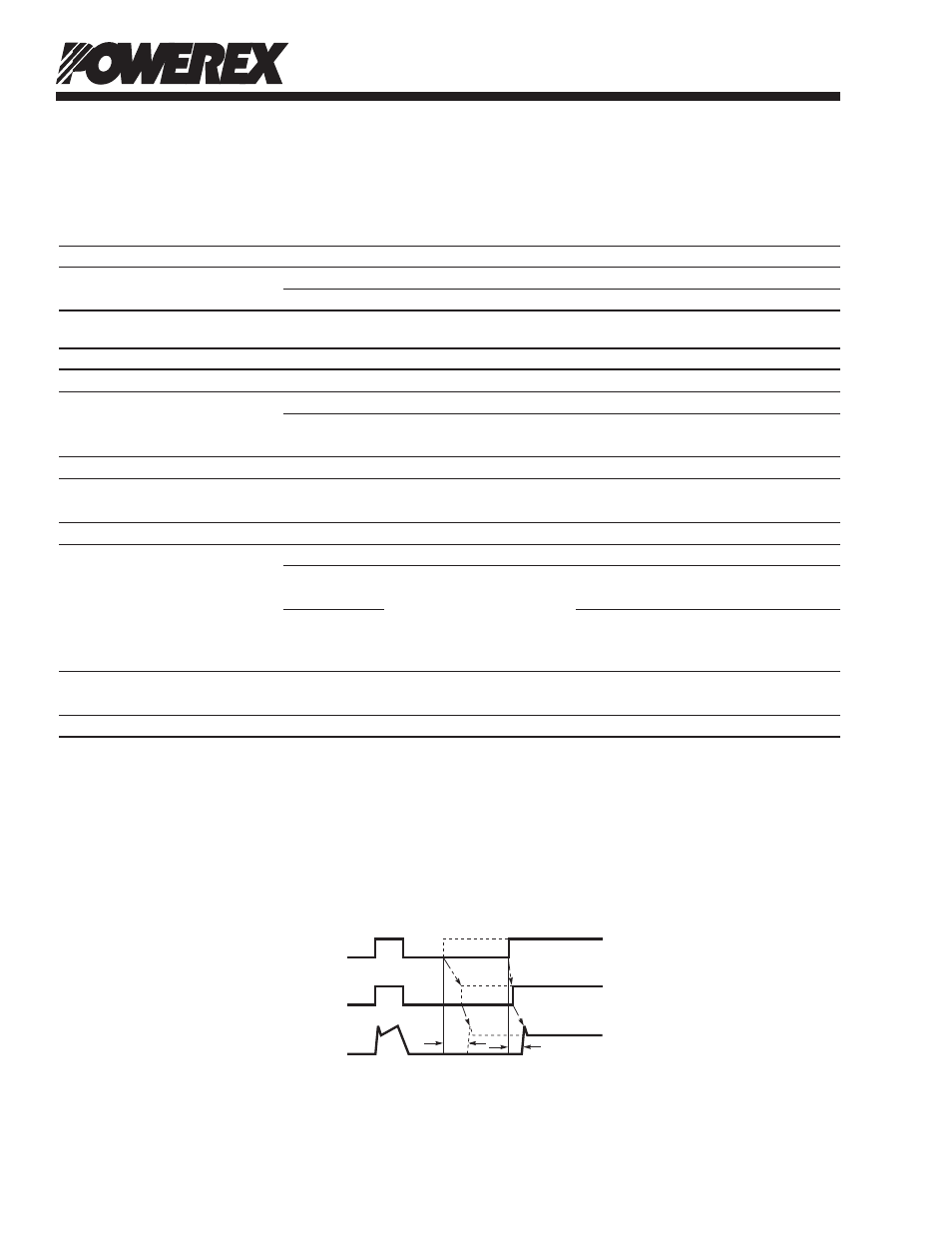
Delayed Response Against Shorter Input OFF Signal than P
WIN(off)
(P-side Only)
t2
t1
P-SIDE
CONTROL INPUT
INTERNAL
IGBT GATE
OUTPUT
CURRENT IC
Solid Line – OFF Pulse Width > PWIN(off): Turn ON time t1.
Dotted Line – OFF Pulse Width < PWIN(off): Turn ON time t2.