Application circuit – C&H Technology PS51789 User Manual
Page 5
PS51789
Intellimod™ Module
Dual-In-Line Intelligent Power Factor Correction Module
30 Amperes/600 Volts
4
03/10 Rev. 0
Powerex, Inc., 173 Pavilion Lane, Youngwood, Pennsylvania 15697 (724) 925-7272 www.pwrx.com
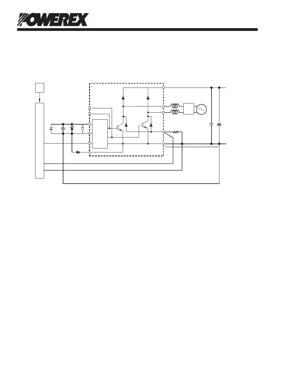
Application Circuit
V
CC
CONTR
OL IC
R
OUT
RG
V
D
V
IN
V
NO
GND
SG
MCU
S
OUT
V
NO
V
IN
A
B
N2
N
C2
C1
+
S
R
P
GND
IGBT1
FWDi4
FWDi3
FWDi2
FWDi1
IGBT2
C4
C3
15V
LINE
NOTE:
1. Due to high speed and large surge voltage switching, the area P-C1-N should be a small as possible. (C1: good temperature,
frequency characteristic electrolytic type). Also add a bypass condenser (C2) with good frequency response such as polypropylene
as close as possible to the P and N terminals.
2. To prevent erroneous protection, the wiring of A, B should be as short as possible.
3. It is recommended to insert a high-speed clamp diode between V
NO
-GND terminals to prevent surge destruction.
4. C3 and C4 capacitors should be mounted as close to the terminals of the DIPPFC as possible. C3, good temperature, frequency
characteristic electrolytic type and C4, good temperature, frequency and DC bias characteristic ceramic type are recommended.
5. It is recommended to insert a Zener diode (24V/1W) between each pair of control supply terminals to prevent surge destruction.
6. Please connect adjacent terminals with the same name together on the PCB. (N, N2, V
NO
, V
IN
, V
D
, S)
7. Do not connect RG and SG terminals to any wire on the PCB.