Vishay semiconductors – C&H Technology VS-GB400AH120N User Manual
Page 5
VS-GB400AH120N
www.vishay.com
Vishay Semiconductors
Revision: 06-Aug-12
4
Document Number: 93483
For technical questions within your region:
,
,
THIS DOCUMENT IS SUBJECT TO CHANGE WITHOUT NOTICE. THE PRODUCTS DESCRIBED HEREIN AND THIS DOCUMENT
ARE SUBJECT TO SPECIFIC DISCLAIMERS, SET FORTH AT
www.vishay.com/doc?91000
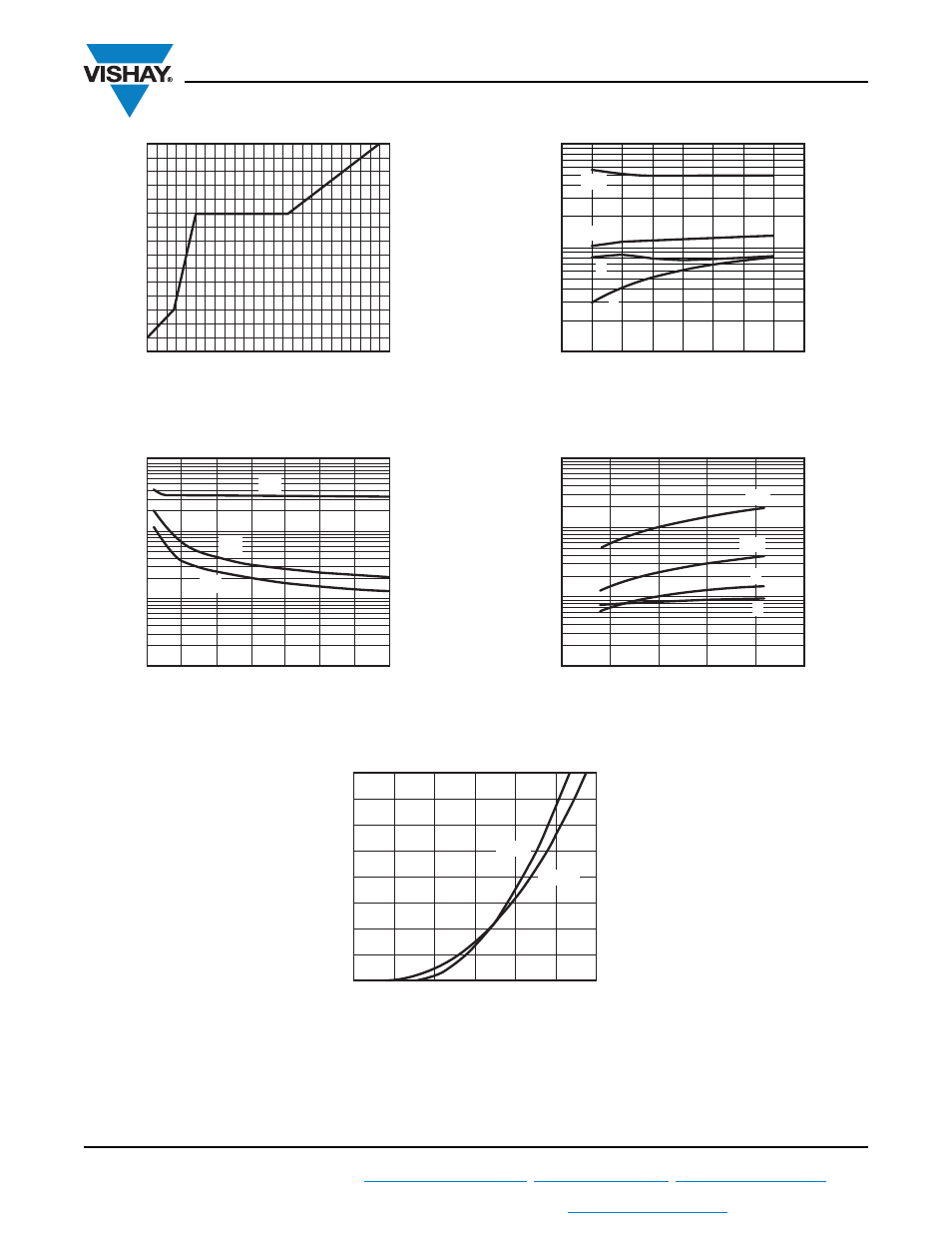
Fig. 5 - Gate Charge Characteristics
V
CC
= 600 V, I
C
= 400 A, T
J
= 25 °C
Fig. 6 - Typical Capacitance vs. Collector to Emitter Voltage
Fig. 7 - Typical Switching Times vs. I
C
V
CC
= 600 V, R
g
= 4
, V
GE
= ± 15 V, T
J
= 125 °C
Fig. 8 - Typical Switching Times vs. Gate Resistance
V
CC
= 600 V, I
C
= 400 A, V
GE
= ± 15 V, T
J
= 125 °C
Fig. 9 - Typical Forward Characteristics (Diode)
V
G
E
(V)
Q
g
(μC)
0
2
1
3
5
4
93483_05
20
10
- 10
0
0.1
1
10
100
0
93483_06
5
15
25
10
20
30
V
CE
(V)
C (nF)
35
C
res
C
ies
C
oes
t (ns)
I
C
(A)
0
800
600
200
400
10
93483_07
1000
100
t
d(off)
t
d(on)
t
f
t
r
t (ns)
R
g
(
Ω)
0
5
10
15
20
25
10
93483_08
10 000
1000
100
t
d(off)
t
d(on)
t
f
t
r
I
F
(A)
V
F
(V)
0
3
1
2
0
93483_09
800
400
200
600
125 °C
25 °C