Vishay semiconductors, Electrical specifications (t, 25 °c unless otherwise specified) – C&H Technology VS-GB90SA120U User Manual
Page 3: Switching characteristics (t, Thermal and mechanical specifications
VS-GB90SA120U
www.vishay.com
Vishay Semiconductors
Revision:02-Aug-12
2
Document Number: 94725
For technical questions within your region:
,
,
THIS DOCUMENT IS SUBJECT TO CHANGE WITHOUT NOTICE. THE PRODUCTS DESCRIBED HEREIN AND THIS DOCUMENT
ARE SUBJECT TO SPECIFIC DISCLAIMERS, SET FORTH AT
www.vishay.com/doc?91000
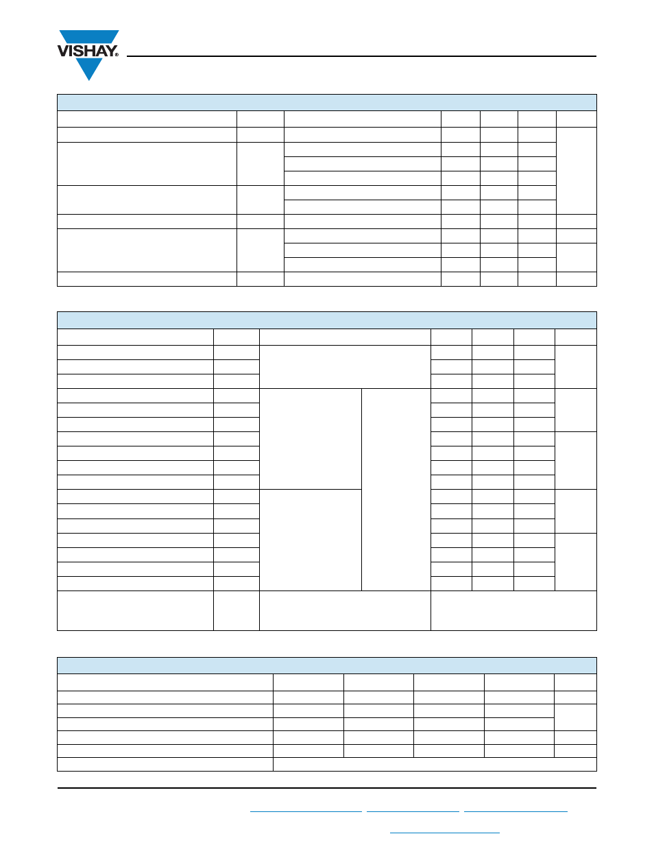
ELECTRICAL SPECIFICATIONS (T
J
= 25 °C unless otherwise specified)
PARAMETER
SYMBOL
TEST CONDITIONS MIN.
TYP.
MAX.
UNITS
Collector to emitter breakdown voltage
V
BR(CES)
V
GE
= 0 V, I
C
= 250 μA
1200
-
-
V
Collector to emitter voltage
V
CE(on)
V
GE
= 15 V, I
C
= 75 A
-
3.3
3.8
V
GE
= 15 V, I
C
= 75 A, T
J
= 125 °C
-
3.6
3.9
V
GE
= 15 V, I
C
= 75 A, T
J
= 150 °C
-
3.7
-
Gate threshold voltage
V
GE(th)
V
CE
= V
GE
, I
C
= 250 μA
4
5
6
V
CE
= V
GE
, I
C
= 250 μA, T
J
= 125 °C
-
3.2
-
Temperature coefficient of threshold voltage V
GE(th)
/
T
J
V
CE
= V
GE
, I
C
= 1 mA (25 °C to 125 °C)
-
- 12
-
mV/°C
Collector to emitter leakage current
I
CES
V
GE
= 0 V, V
CE
= 1200 V
-
7
250
μA
V
GE
= 0 V, V
CE
= 1200 V, T
J
= 125 °C
-
1.4
10
mA
V
GE
= 0 V, V
CE
= 1200 V, T
J
= 150 °C
-
6.5
20
Gate to emitter leakage current
I
GES
V
GE
= ± 20 V
-
-
± 250
nA
SWITCHING CHARACTERISTICS (T
J
= 25 °C unless otherwise specified)
PARAMETER
SYMBOL
TEST CONDITIONS MIN.
TYP.
MAX.
UNITS
Total gate charge (turn-on)
Q
g
I
C
= 50 A, V
CC
= 600 V, V
GE
= 15 V
-
690
-
nC
Gate to emitter charge (turn-on)
Q
ge
-
65
-
Gate to collector charge (turn-on)
Q
gc
-
250
-
Turn-on switching loss
E
on
I
C
= 75 A, V
CC
= 600 V,
V
GE
= 15 V, R
g
= 5
L = 500 μH, T
J
= 25 °C
Energy losses
include tail and
diode recovery
Diode used
HFA16PB120
-
1.2
-
mJ
Turn-off switching loss
E
off
-
2.1
-
Total switching loss
E
tot
-
3.3
-
Turn-on delay time
t
d(on)
-
250
-
ns
Rise time
t
r
-
38
-
Turn-off delay time
t
d(off)
-
280
-
Fall time
t
f
-
90
-
Turn-on switching loss
E
on
I
C
= 75 A, V
CC
= 600 V,
V
GE
= 15 V, R
g
= 5
L = 500 μH, T
J
= 125 °C
-
1.7
-
mJ
Turn-off switching loss
E
off
-
4.08
-
Total switching loss
E
tot
-
5.78
-
Turn-on delay time
t
d(on)
-
245
-
ns
Rise time
t
r
-
48
-
Turn-off delay time
t
d(off)
-
280
-
Fall time
t
f
-
140
-
Reverse bias safe operating area
RBSOA
T
J
= 150 °C, I
C
= 200 A, R
g
= 22
V
GE
= 15 V to 0 V, V
CC
= 900 V,
V
P
= 1200 V, L = 500 μH
Fullsquare
THERMAL AND MECHANICAL SPECIFICATIONS
PARAMETER
SYMBOL
MIN. TYP. MAX.
UNITS
Maximum junction and storage temperature range
T
J
, T
Stg
- 40
-
150
°C
Junction to case thermal resistance
IGBT
R
thJC
-
-
0.145
°C/W
Case to sink thermal resistance, flat, greased surface
R
thCS
-
0.1
-
Mounting torque, on terminals and heatsink
-
-
1.3
Nm
Weight
-
30
-
g
Case style
SOT-227