Vishay semiconductor italy, Electrical characteristics @ t, 25°c (unless otherwise specified) – C&H Technology GB100DA60UP User Manual
Page 3: Switching characteristics @ t
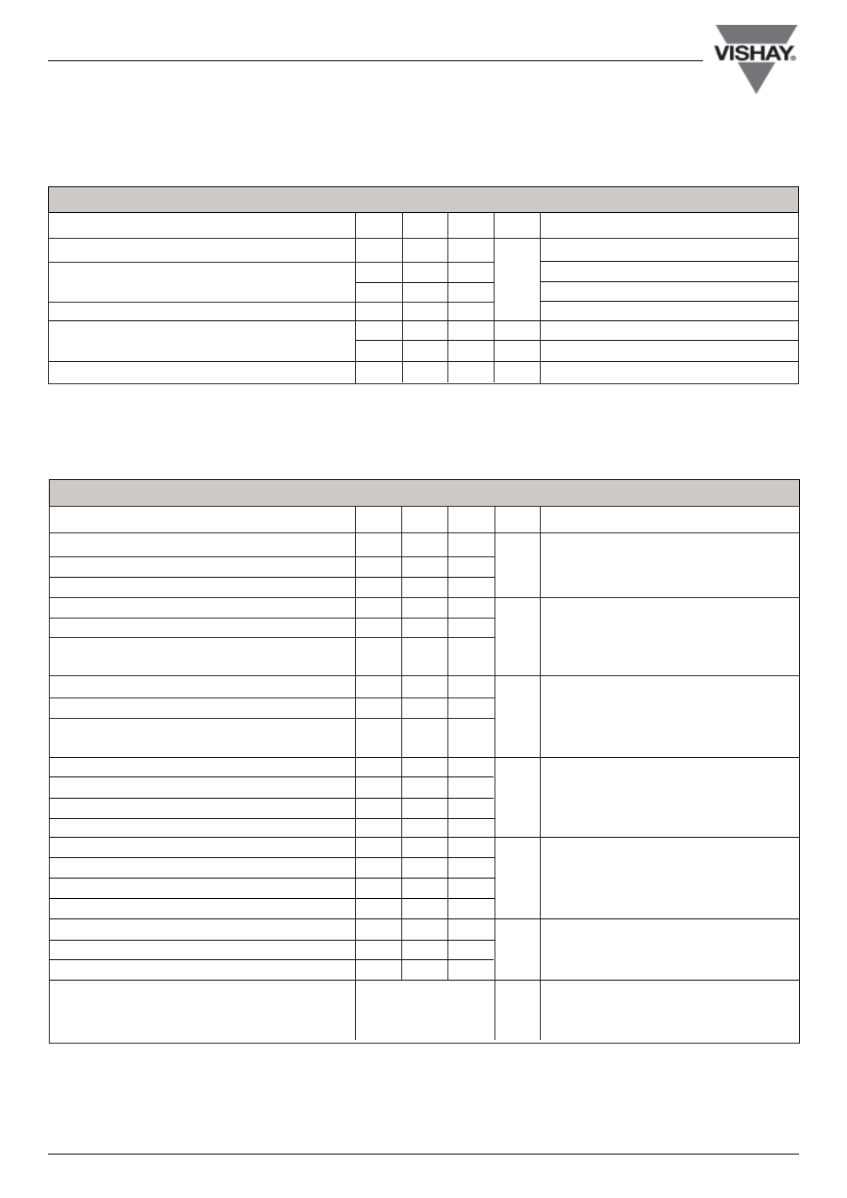
GB100DA60UP
Vishay Semiconductor Italy
2
Revision 28-Mar-08
V
(BR)CES
Collector-to-Emitter Breakdown Voltage
600
V
V
GE
= 0V, I
C
= 500μA
V
CE(on)
Collector-to-Emitter Voltage
2.4
V
GE
= 15V, I
C
= 100A
3
V
GE
= 15V, I
C
= 100A, T
J
= 125°C
V
GE(th)
Gate Threshold Voltage
4
I
C
= 0.5mA
I
CES
Collector-to-Emiter Leaking
7
μA
V
GE
= 0V, V
CE
= 600V
Current
4
mA
V
GE
= 0V, V
CE
= 600V, T
J
= 150°C
I
GES
Gate-to-Emitter Leakage Current
± 200
nA
V
GE
= ± 20V
PARAMETERS
MIN
TYP
MAX UNITS TEST CONDITIONS
Q
g
Total Gate Charge (turn-on)
460
690
nC
I
C
= 100A
Q
ge
Gate-Emitter Charge (turn-on)
160
250
V
CC
= 480V
Q
gc
Gate-Collector Charge (turn-on)
70
130
V
GE
= 15V
E
on
Turn-On Switching Loss
360
μJ
R
G
= 5
Ω
E
off
Turn-Off Switching Loss
1420
I
C
= 100A, V
CC
= 360V, V
GE
= 15V, L = 500μH
E
ts
Total Switching Loss
1780
Energy losses include tail and diode reverse
recovery
E
on
Turn-On Switching Loss
520
μJ
R
G
= 5
Ω
E
off
Turn-Off Switching Loss
1600
I
C
= 100A, V
CC
= 360V, V
GE
= 15V, L = 500μH
E
ts
Total Switching Loss
2120
Energy losses include tail and diode reverse
recovery,
T
J
= 125°C
td
on
Turn-On Delay Time
260
ns
R
G
= 5
Ω
t
r
Rise Time
53
I
C
= 100A, V
CC
= 360V, V
GE
= 15V, L = 500μH
td
off
Turn-Off Delay Time
248
Energy losses include tail and diode reverse
t
f
Fail Time
76
recovery
td
on
Turn-On Delay Time
264
ns
R
G
= 5
Ω
t
r
Rise Time
54
I
C
= 100A, V
CC
= 360V, V
GE
= 15V, L = 500μH
td
off
Turn-Off Delay Time
254
Energy losses include tail and diode reverse
t
f
Fail Time
80
recovery,
T
J
= 125°C
C
ies
Input Capacitance
8000
pF
V
GE
= 0V
C
oes
Output Capacitance
790
V
CC
= 30V
C
res
Reverse Transfer Capacitance
110
f = 1.0 MHz
RBSOA Reverse Bias Safe Operating Area
full square
T
J
= 150°C, I
C
= 300A
V
CC
= 400V, V
P
= 600V
R
G
= 22
Ω, V
GE
= +15V to 0V
ELECTRICAL CHARACTERISTICS @ T
J
= 25°C
(unless otherwise specified)
PARAMETERS
MIN
TYP
MAX UNITS TEST CONDITIONS
SWITCHING CHARACTERISTICS @ T
J
= 25°C
(unless otherwise specified)