Protection function timing diagrams – C&H Technology PS22053 User Manual
Page 8
PS22053
Intellimod™ Module
Dual-In-Line Intelligent Power Module
10 Amperes/1200 Volts
Powerex, Inc., 200 E. Hillis Street, Youngwood, Pennsylvania 15697-1800 (724) 925-7272
7
Rev. 10/05
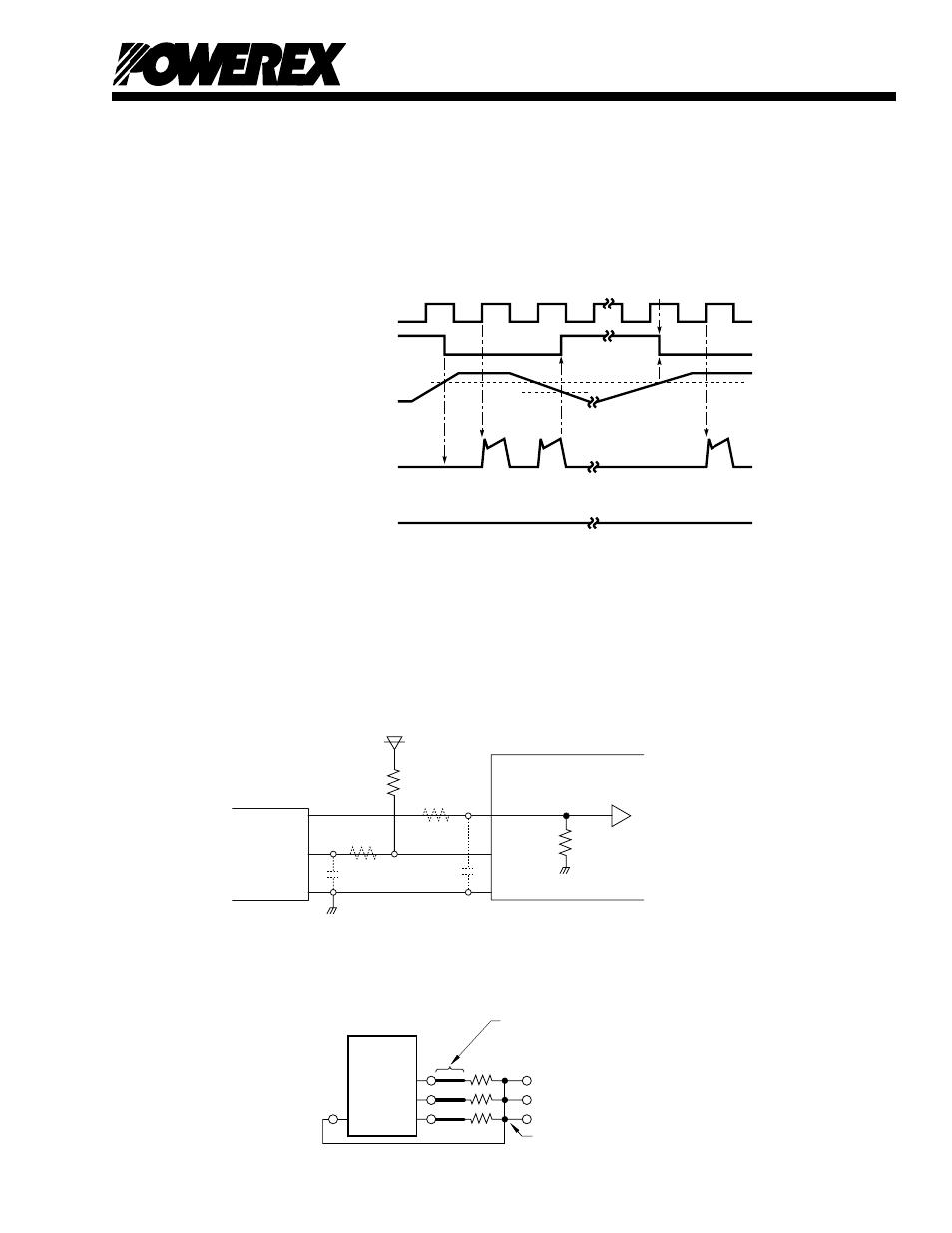
Protection Function Timing Diagrams
C1
C4
C5
C2
UVDt
C6
C3
SET
RESET
RESET
HIGH LEVEL MEANS NO FO OUTPUT
UVDBr
CONTROL INPUT
PROTECTION
CIRCUIT STATE
CONTROL SUPPLY
VOLTAGE VDB
OUTPUT CURRENT IC
FAULT OUTPUT FO
Under-Voltage Protection (P-side, UVDB)
C1: Control supply voltage rises – After the voltage level reaches UVDBr, the drive circuit begins to work
at the rising edge of the next input signal.
C2: Normal operation – IGBT turn on and conducting current.
C3: Under-voltage trip (UVDBt).
C4: IGBT stays off regardless of the control input level, but there is no FO signal output.
C5: Under-voltage reset (UVDr).
C6: Normal operation – IGBT turn on and conducting current.
Typical Interface Circuit
Wiring Method Around Shunt Resistor
RSHUNT (Chip type resistor is recommended.)
VNC
NW
NV
NU
DIP-IPM
Wiring inductance should be less than 10nH.
This GND wiring from VNC should be as
close to the shunt resistors as possible.
UP, VP, WP, UN, VN, WN
MCU
5V LINE
10k
Ω
2.5k
Ω (MIN)
FO
VNC (LOGIC)
DIP-IPM
NOTE: RC coupling at each input
(parts shown dotted) may change
depending on the PWM control
scheme used in the application
and the wiring impedance of the
printed circuit board. The DIP-IPM
input signal section integrates a
2.5k
Ω (min) pull-down resistor.
Therefore, when using an external
filtering resistor, care must be
taken to satisfy the turn-on
threshold voltage requirement.