Cpv364m4kpbf, Vishay high power products – C&H Technology CPV364M4KPbF User Manual
Page 4
Document Number: 94488
For technical questions, contact: [email protected]
www.vishay.com
Revision: 01-Sep-08
3
CPV364M4KPbF
IGBT SIP Module
(Short Circuit Rated
Ultrafast IGBT)
Vishay High Power Products
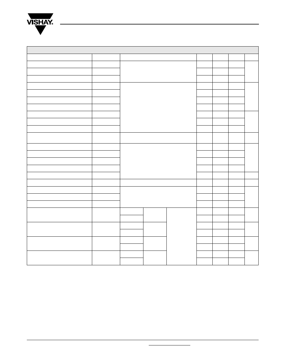
SWITCHING CHARACTERISTICS (T
J
= 25 °C unless otherwise specified)
PARAMETER SYMBOL
TEST
CONDITIONS
MIN.
TYP.
MAX.
UNITS
Total gate charge (turn-on)
Q
g
I
C
= 13 A
V
CC
= 400 V
V
GE
= 15 V
See fig. 8
-
110
170
nC
Gate to emitter charge (turn-on)
Q
ge
-
14
21
Gate to collector charge (turn-on)
Q
gc
-
49
74
Turn-on delay time
t
d(on)
T
J
= 25 °C
I
C
= 13 A, V
CC
= 480 V
V
GE
= 15 V, R
G
= 10
Ω
Energy losses include “tail” and diode
reverse recovery
See fig. 9, 10, 18
-
50
-
ns
Rise time
t
r
-
30
-
Turn-off delay time
t
d(off)
-
110
170
Fall time
t
f
-
91
140
Turn-on switching loss
E
on
-
0.56
-
mJ
Turn-off switching loss
E
off
-
0.28
-
Total switching loss
E
ts
-
0.84
1.1
Short circuit withstand time
t
sc
V
CC
= 360 V,T
J
= 125 °C
V
GE
= 15 V, R
G
= 10
Ω, V
CPK
< 500 V
10
-
-
µs
Turn-on delay time
t
d(on)
T
J
= 150 °C, see fig. 9, 10, 11, 18
I
C
= 13 A, V
CC
= 480 V
V
GE
= 15 V, R
G
= 10
Ω
Energy losses include “tail” and
diode reverse recovery
-
47
-
ns
Rise time
t
r
-
30
-
Turn-off delay time
t
d(off)
-
250
-
Fall time
t
f
-
150
-
Total switching loss
E
ts
-
1.28
-
mJ
Internal emitter inductance
L
E
Measured 5 mm from package
-
7.5
-
nH
Input capacitance
C
ies
V
GE
= 0 V
V
CC
= 30 V
ƒ = 1.0 MHz
See fig. 7
-
1600
-
pF
Output capacitance
C
oes
-
130
-
Reverse transfer capacitance
C
res
-
55
-
Diode reverse recovery time
t
rr
T
J
= 25 °C
See fig. 14
I
F
= 15 A
V
R
= 200 V
dI/dt = 200 A/µs
-
42
60
ns
T
J
= 125 °C
-
74
120
Diode peak reverse recovery charge
I
rr
T
J
= 25 °C
See fig. 15
-
4.0
6.0
A
T
J
= 125 °C
-
6.5
10
Diode reverse recovery charge
Q
rr
T
J
= 25 °C
See fig. 16
-
80
180
nC
T
J
= 125 °C
-
220
600
Diode peak rate of fall of recovery
during t
b
dI
(rec)M
/dt
T
J
= 25 °C
See fig. 17
-
188
-
A/µs
T
J
= 125 °C
-
160
-