2 device fault reporting – Texas Instruments TAS5121 User Manual
Page 23
Device Fault Reporting
3-3
Protection
3.2 Device Fault Reporting
The OTW and SD outputs from the TAS5121 indicate fault conditions. See the
TAS5121 data sheet (SLES086) for a description of these pins.
The temperature warning signals at the TAS5508−5121K8EVM board are
wired-OR to one temperature warning signal [OTW – pin 22 in control interface
connector (J30)].
Shutdown signals are wired-OR into two shutdown signals [SD1 and SD2 – pin
20 and pin 21 in control interface connector (J30)]. See Table 3−1 for channel
allocation.
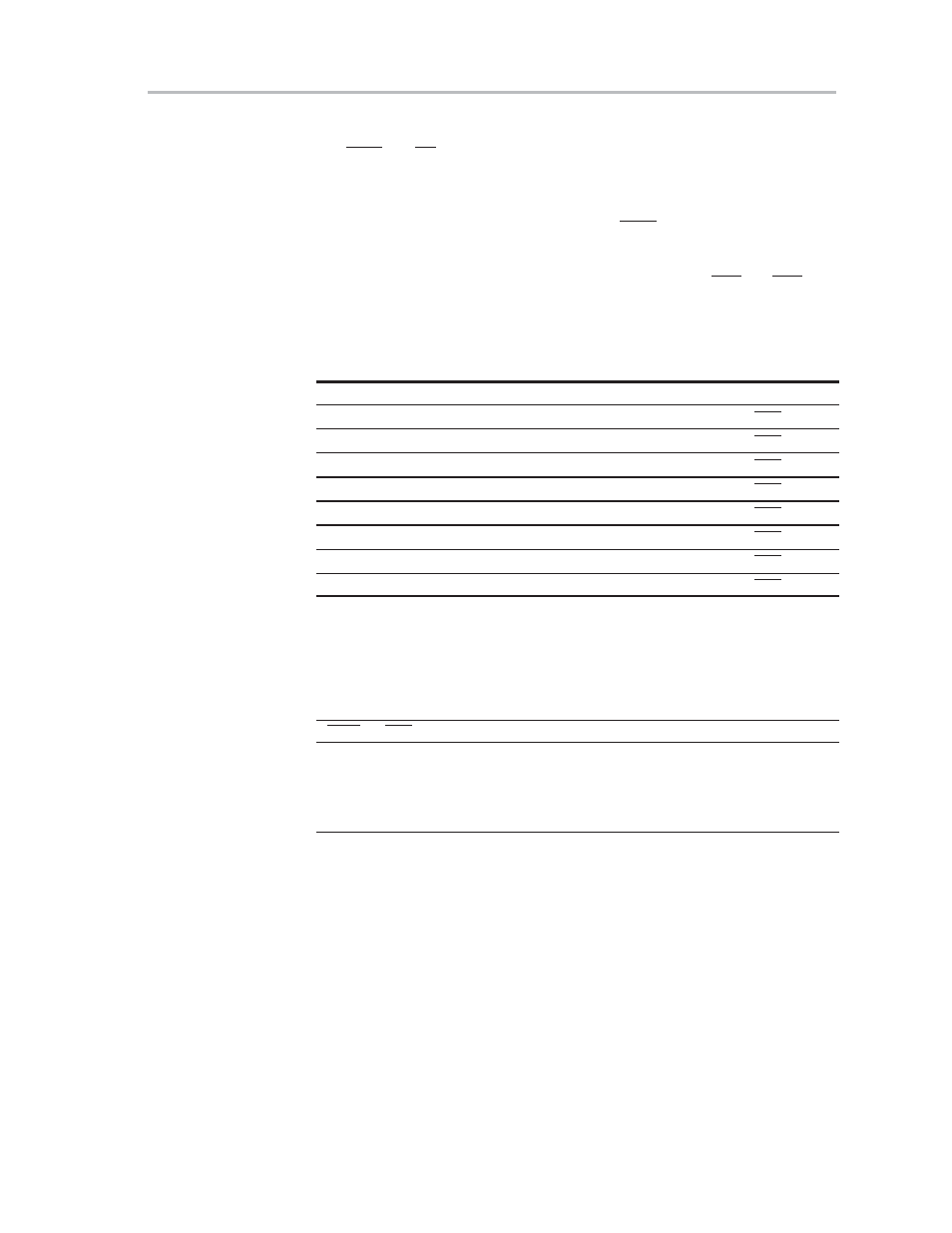
Table 3−1. Channel Allocation
Description
Terminal
Shutdown Signal
Front left
J100
SD1
Front right
J200
SD1
Rear left
J300
SD2
Rear right
J400
SD2
Surround left (or line out left)
J500
SD2
Surround right (or line out right)
J600
SD2
Center
J700
SD1
Subwoofer
J800
SD2
The shutdown signals, together with the temperature warning signal, give chip
state information as described in Table 3−2. Device fault reporting outputs are
open-drain outputs.
Table 3−2. TAS5121 Warning/Error Signal Decoding
OTW
SDx
Device Condition
0
0
High-temperature error and/or high-current error
0
1
High-temperature warning
1
0
Undervoltage lockout or high-current error
1
1
Normal operation, no errors/warnings