Texas Instruments TAS5121 User Manual
Page 15
Power Supply (PSU) Interface (J70, J71, and J73)
2-3
System Interfaces
Table 2−2. J71 Pin Description
Pin No.
Net-Name at Schematics
Description
1
V-HBRIDGE
Output-stage power supply
2
−
System power supply
3
GND
Ground
4
GND
Ground
Table 2−3. J70 Pin Description
(Optional − Use to decrease of impedance to reach better performance)
Pin No.
Net-Name at Schematics
Description
1
V-HBRIDGE
Extra output-stage power supply
2
V-HBRIDGE
Extra output-stage power supply
3
GND
Extra ground
4
GND
Extra ground
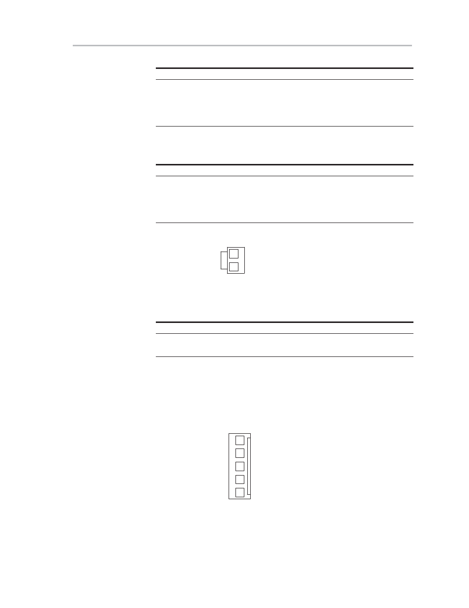
Figure 2−3. J73 Pin Numbers
1
2
(PCB connector top view)
Table 2−4. J73 Pin Description
(Optional)
Pin No.
Net-Name at Schematics
Description
1
V-HBRIDGE
Extra output-stage power supply
2
V-HBRIDGE
Extra output-stage power supply
2.1.1 PSU Control Interface (J72)
This interface is used for onboard sensing of output supply voltage and for the
power supply volume control (PSVC) signal.
Figure 2−4. J72 Pin Numbers
1
2
3
5
4
(PCB connector top view)