Typical application 2, Rv5vh3 – Ricoh RV5VH User Manual
Page 46
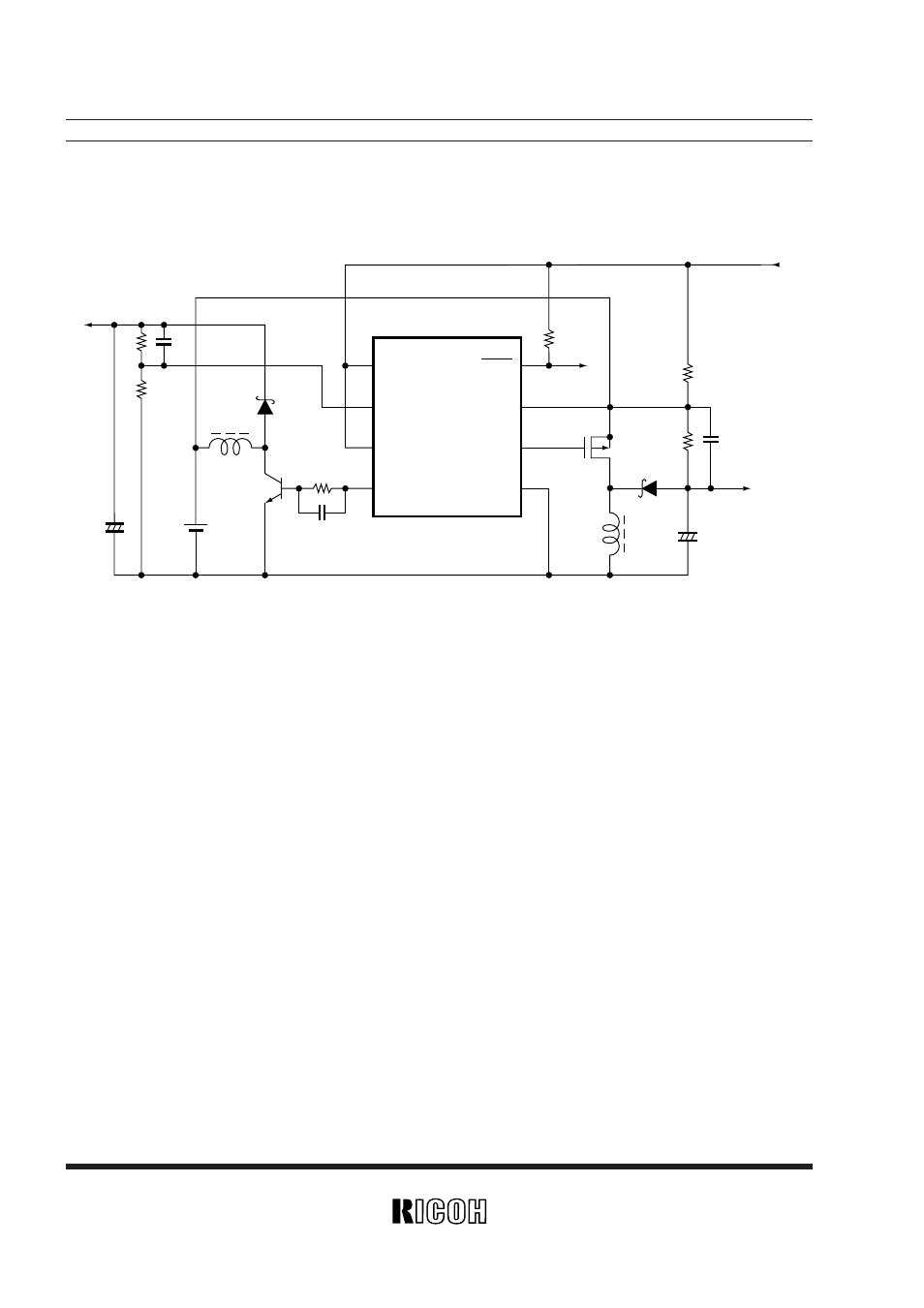
RV5VH3
××
42
CSW
FB1
V
DD
EXT1
D
OUT
FB2
EXT2
GND
C2
L2
PMOS
R3
R1
V
IN
R2
C3
SBD
C1
NPN Tr.
SBD
R6
R4
C4
R5
C5
L1
Output DC/DC 2
Output DC/DC 1
TYPICAL APPLICATION 2
CoiI
L1 : 100µH, L2 : 100µH
Diode
Schottky type
capacitor
C1 : 22µF(Ta), C2 : 22µF(Ta)
C3 : 0.01µF (ceramic)
C4 : 0.01µF (ceramic)
C5 : 0.01µF (ceramic)
PMOS
2SJ238 (TOSHIBA)
NPN Tr.
2SD1628G (SANYO)
Resistor
R1 : 100K
Ω
, R2 : 0 to 500K
Ω
R3 : 100K
Ω
R4 : 300
Ω
R5 : 0 to 500K
Ω,
R6 : 50K
Ω
Description
• Step up DC/DC converter : DC/DC1
The oscillator can operate when CSW is “H”. When the CSW is “L” the EXT1 outputs GND.
The output voltage can be adjusted by R5 and R6 with FB1 of two volt.
• Invering DC/DC converter : DC/DC2
The oscillator can operate when CSW is “H”. When the CSW is “L” the EXT2 outputs V
DD
.
The output voltage can be adjusted by R1 and R2 with FB2 of zero volt.
• VoItage Detector
V
DD
pin can be monitored. This could be operated all the time by V
DD
.
The D
OUT
pin outputs “L” when low voltage is detected with Nch open-drain output.