Ricoh RV5VH User Manual
Page 23
19
RV5VH1
××
/RV5VH2
××
C1
L
FB
V
OUT2
V
OUT1
EXT2
+
–
RV5VH1
××
/RV5VH2
××
Error Amp.2
VFM2
CSW
6
1
7
SBD
+
PMOS
OSC
C2
R2
R1
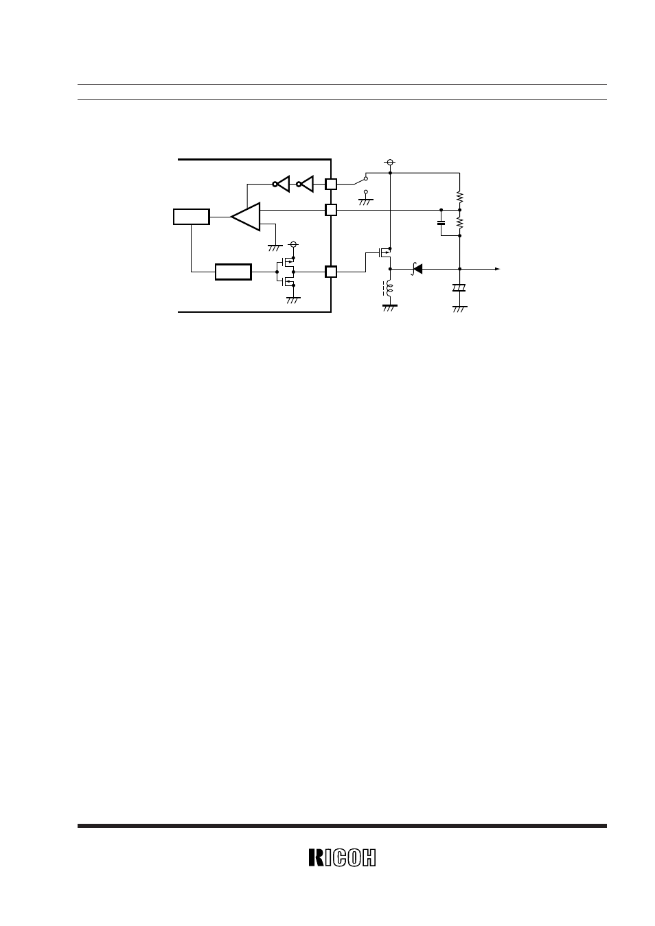
The DC/DC2 can operate by a voltage of “V
OUT1
”. A change in the V
OUT2
will feed back to the internal error amplifier
through external voltage setting resistors. The reference voltage should be provided from externally fixed power supply
such as V
OUT1
.
When the feed back voltage to the cmp2 is higher than the ground voltage the error amplifier enables oscillation or other-
wise will stop oscillation.
Pulses from the “OSC” circuit have a duty cycle of 50% and it makes VFM operation allowable. There might be certain cas-
es that the duty cycles becomes smaller temporally at light load current. The output of “EXT2” is driven by CMOS buffer
operated V
OUT1
and GND.
A PMOS driver will be connected to the “EXT2” pin and its switching operation generates negative output voltage through
energy accumulated in an inductor.
The DC/DC1 can be shut down by CSW pin. When the CSW pin is High, V
DD
level, the DC/DC1 is enabled and when the
CSW pin is Low, GND level, the DC/DC1 is disabled. The EXT2 pin outputs High while the DC/DC2 is disabled.
• Set output voltage DC/DC Converter2
V
OUT2
is described as follows:
V
OUT1
:R1=|–V
OUT2
| : R2
/ The FB voltage is controlled to 0V and V
OUT1
is provided externally
|–V
OUT2
|=V
OUT1
×
R2/R1
so any output voltage of DC/DC2 can be set by changing R1 or/and R2.
Certain temperature coefficient of V
OUT2
can be set by using R1,R2 having such temperature characteristics.
• DC/DC Converter 2