National Products DS90C3202 User Manual
General description, Features, Block diagram
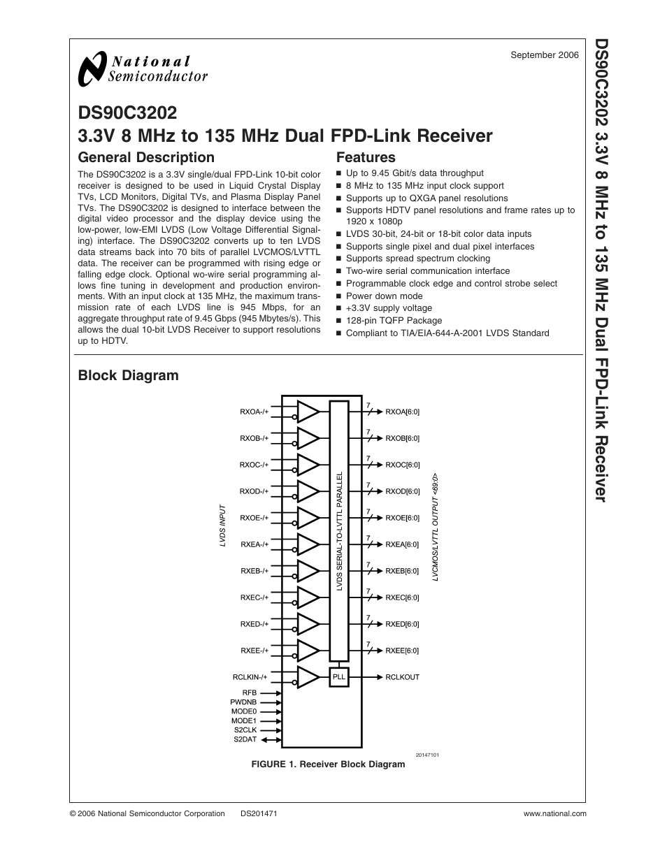
Table of contents
Document Outline
- DS90C3202
- General Description
- Features
- Block Diagram
- Typical Application Diagram
- Functional Description
- Absolute Maximum Ratings
- Recommended Operating Conditions
- Electrical Characteristics
- Receiver Switching Characteristics
- Two-Wire Serial Communication Interface
- AC Timing Diagrams
- FIGURE 1. Two-Wire Serial Communication Interface Timing Diagram
- FIGURE 2. "Worst Case" Test Pattern
- FIGURE 3. Incremental Test Pattern
- FIGURE 4. Typical and Max ICC with Worse Case and Incremental Pattern
- FIGURE 5. LVCMOS/LVTTL Output Load and Transition Times
- FIGURE 6. Receiver Phase Lock Loop Wake-up Time
- FIGURE 7. Powerdown Delay
- FIGURE 8. Receiver Propagation Delay
- FIGURE 9. RFB: LVTTL Level Programmable Strobe Select
- FIGURE 10. Receiver Input Tolerance and Sampling Window
- FIGURE 11. Receiver RSRC and RHRC Output Setup/Hold Time - PTO Disabled
- FIGURE 12. Receiver RSRC and RHRC Output Setup/Hold Time - PTO Enabled
- FIGURE 13. Receiver RSRC and RHRC Output Setup/Hold Time Adjustment - PTO Disabled
- FIGURE 14. Receiver RSRC and RHRC Output Setup/Hold Time Adjustment - PTO Enabled
- FIGURE 15. LVDS Input Mapping
- FIGURE 16. Receiver RITOL Min and Max
- Pin Diagram
- DS90C3202 Pin Descriptions
- Two-Wire Serial Communication Interface Description
- FIGURE 17. Byte Read
- FIGURE 18. Byte Write
- DS90C3202 Two-Wire Serial Interface Register Table
- Physical Dimensions