National Products DS90C3202 User Manual
General description, Features, Block diagram
DS90C3202
3.3V 8 MHz to 135 MHz Dual FPD-Link Receiver
General Description
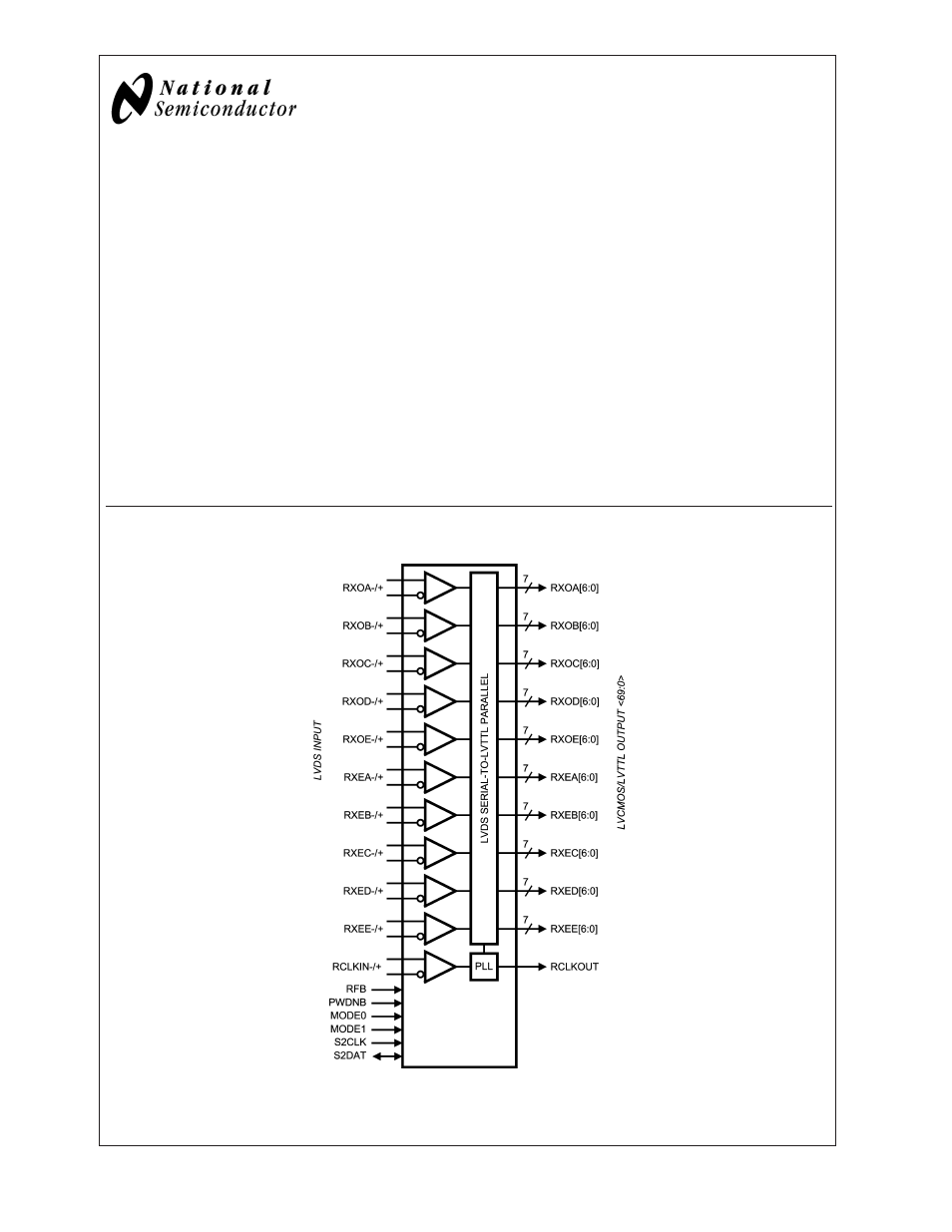
The DS90C3202 is a 3.3V single/dual FPD-Link 10-bit color
receiver is designed to be used in Liquid Crystal Display
TVs, LCD Monitors, Digital TVs, and Plasma Display Panel
TVs. The DS90C3202 is designed to interface between the
digital video processor and the display device using the
low-power, low-EMI LVDS (Low Voltage Differential Signal-
ing) interface. The DS90C3202 converts up to ten LVDS
data streams back into 70 bits of parallel LVCMOS/LVTTL
data. The receiver can be programmed with rising edge or
falling edge clock. Optional wo-wire serial programming al-
lows fine tuning in development and production environ-
ments. With an input clock at 135 MHz, the maximum trans-
mission rate of each LVDS line is 945 Mbps, for an
aggregate throughput rate of 9.45 Gbps (945 Mbytes/s). This
allows the dual 10-bit LVDS Receiver to support resolutions
up to HDTV.
Features
n
Up to 9.45 Gbit/s data throughput
n
8 MHz to 135 MHz input clock support
n
Supports up to QXGA panel resolutions
n
Supports HDTV panel resolutions and frame rates up to
1920 x 1080p
n
LVDS 30-bit, 24-bit or 18-bit color data inputs
n
Supports single pixel and dual pixel interfaces
n
Supports spread spectrum clocking
n
Two-wire serial communication interface
n
Programmable clock edge and control strobe select
n
Power down mode
n
+3.3V supply voltage
n
128-pin TQFP Package
n
Compliant to TIA/EIA-644-A-2001 LVDS Standard
Block Diagram
20147101
FIGURE 1. Receiver Block Diagram
September 2006
DS90C3202
3.3V
8
MHz
to
135
MHz
Dual
FPD-Link
Receiver
© 2006 National Semiconductor Corporation
DS201471
www.national.com
Document Outline
- DS90C3202
- General Description
- Features
- Block Diagram
- Typical Application Diagram
- Functional Description
- Absolute Maximum Ratings
- Recommended Operating Conditions
- Electrical Characteristics
- Receiver Switching Characteristics
- Two-Wire Serial Communication Interface
- AC Timing Diagrams
- FIGURE 1. Two-Wire Serial Communication Interface Timing Diagram
- FIGURE 2. "Worst Case" Test Pattern
- FIGURE 3. Incremental Test Pattern
- FIGURE 4. Typical and Max ICC with Worse Case and Incremental Pattern
- FIGURE 5. LVCMOS/LVTTL Output Load and Transition Times
- FIGURE 6. Receiver Phase Lock Loop Wake-up Time
- FIGURE 7. Powerdown Delay
- FIGURE 8. Receiver Propagation Delay
- FIGURE 9. RFB: LVTTL Level Programmable Strobe Select
- FIGURE 10. Receiver Input Tolerance and Sampling Window
- FIGURE 11. Receiver RSRC and RHRC Output Setup/Hold Time - PTO Disabled
- FIGURE 12. Receiver RSRC and RHRC Output Setup/Hold Time - PTO Enabled
- FIGURE 13. Receiver RSRC and RHRC Output Setup/Hold Time Adjustment - PTO Disabled
- FIGURE 14. Receiver RSRC and RHRC Output Setup/Hold Time Adjustment - PTO Enabled
- FIGURE 15. LVDS Input Mapping
- FIGURE 16. Receiver RITOL Min and Max
- Pin Diagram
- DS90C3202 Pin Descriptions
- Two-Wire Serial Communication Interface Description
- FIGURE 17. Byte Read
- FIGURE 18. Byte Write
- DS90C3202 Two-Wire Serial Interface Register Table
- Physical Dimensions