2 data input output specifications, 1 voltage levels, 2 i/o surface mount pads – Navman LA000508 User Manual
Page 11: Table 4‑3: interface voltage levels, Table 4‑4: j20d receiver pad functions

11
LA000507G © 2006 Navman New Zealand. All rights reserved. Proprietary information and specifications subject to change without notice.
4.2 Data input output specifications
All communications between the Jupiter 20 receiver and external devices are through the I/O
surface mount pads. These provide the contacts for power, ground, serial I/O and control. Power
requirements are discussed in Section 4.1.
4.2.1 Voltage levels
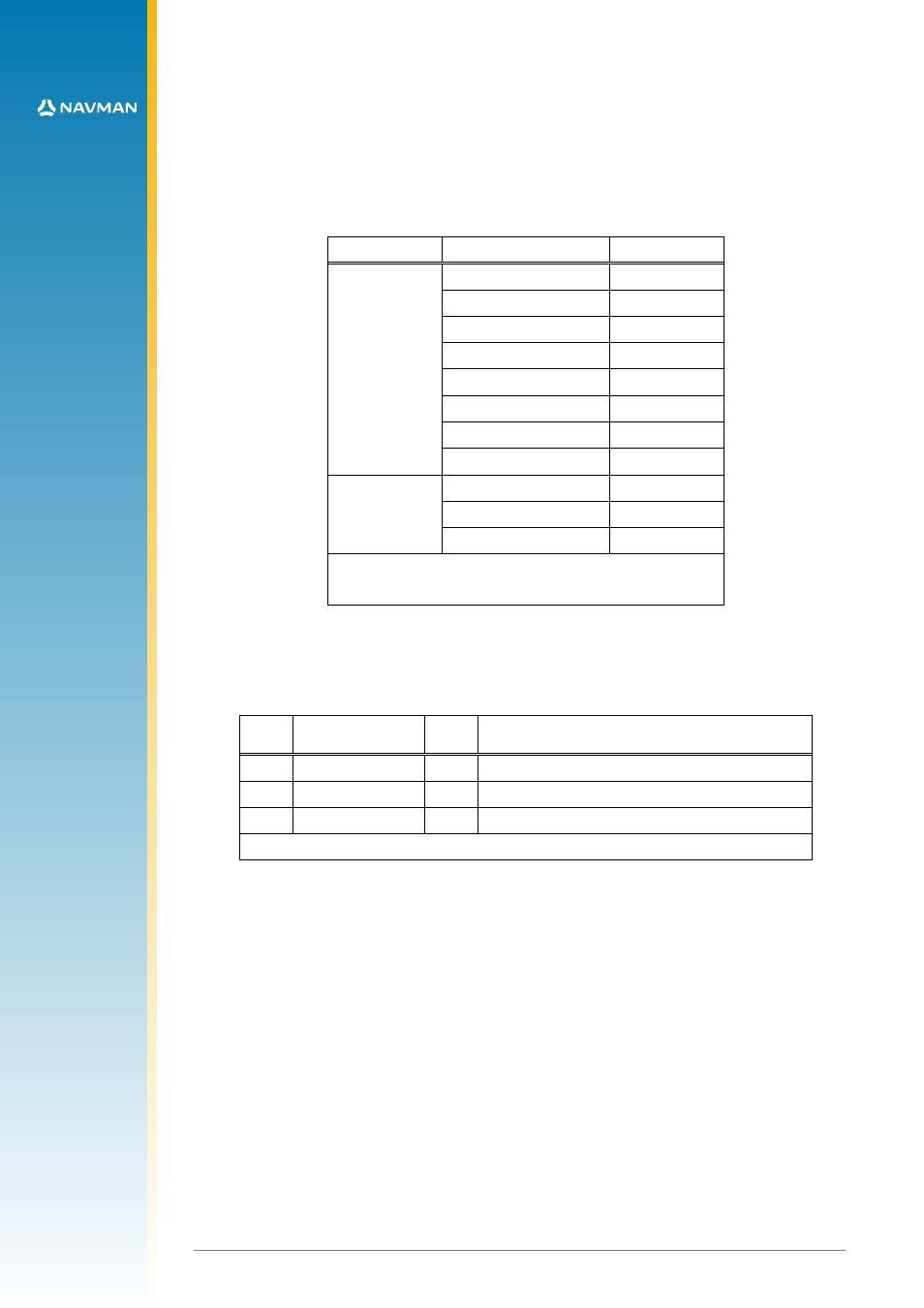
The I/O connector voltage levels measured at PWR_IN = 3 V are shown in Table 4‑3.
Signal
Parameter
Value
TXD & RXD
GPIOs
SPI bus
V
IH
(min)
2.0 V
V
IH
(max)
PWR_IN +0.1 V
V
IL
(min)
0.1 V
V
IL
(max)
0.8 V
V
OH
(min) at
I
OH
2 mA
2.0 V
V
OH
(max)
PWR_IN
V
OL
(min)
0
V
OL
(max) at
I
OL
–2 mA
1.0 V
Reset input*
max capacitance Cmax
100 pF
input current max
–600 μA
pulse time min
200 μs
*Reset input should not be driven high by external circuits. It
is recommended that this input is driven low by an open drain
interface.
Table 4-3: Interface voltage levels
4.2.2 I/O surface mount pads
Details of the surface mount pad functions are shown in Table 4‑4 and 4‑5.
Pad
No.
Name
Type
Description
8*
GYRO_IN
I
gyro input (analogue 0–5 V)
27*
FWD/REV
I
fwd/rev input (low=forward, high=reverse)
28*
WHEEL_TICKS
I
wheel tick input
* See also Table ‑ for J20/J20S pad functions
Table 4-4: J20D receiver pad functions
