Receive buffer register – National Instruments GPIB-COM User Manual
Page 30
Section Five
Programming the GPIB-COM
© National Instruments Corporation
5-3
GPIB-COM User Manual
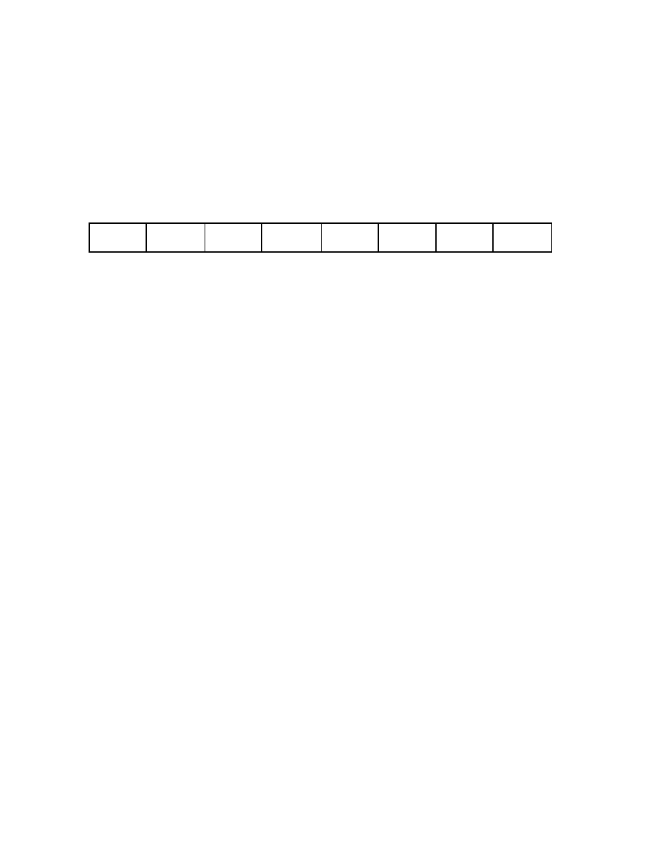
Receive Buffer Register
Offset from Base I/O Address = 0
Register Address = XF8
DLAB bit in Line Control Register = 0
7
6
5
4
3
2
1
0
D6
D5
D7
D4
D3
D2
D1
D0
R
The Receive Buffer Register contains the character received from the serial input, with bit 0 being
the least significant and bit 7 the most significant. It functions identically on the GPIB-COM and
the INS8250.
Bit
Mnemonic
Description
7-0r
D[7-0]
Data Bits 7 through 0
See also other documents in the category National Instruments Computer Accessories:
- R Series Intelligent DAQ PXI-784xR (14 pages)
- 7344 (66 pages)
- Relay Module SCC-RLY01 (9 pages)
- Compact FieldPoint Mounting Accessories cFP-21xx (10 pages)
- PCI-4451 (115 pages)
- NI 6239 (172 pages)
- SCXI-1190 (54 pages)
- SCXI-1190/1191 (45 pages)
- NI 785xR (74 pages)
- DIO 6533 (125 pages)
- Multisystem eXtension Interface NI PCIe-836x (37 pages)
- GPIB-BUF (40 pages)
- 6527 (47 pages)
- PCI-8336 (43 pages)
- PXI NI PXI-8105 (73 pages)
- 6025E (136 pages)
- NI 78xxR (12 pages)
- PCI-6110E/6111E (113 pages)
- NI 6115/6120 (127 pages)
- 1128 (97 pages)
- 800 Series (104 pages)
- NI 6115 (127 pages)
- NI 784xR (74 pages)
- GPIB-100A (43 pages)
- VXI-MIO Series (151 pages)
- Low-Cost Multifunction I/O Board for ISA Lab-PC+ (211 pages)
- PC-DIO-24/PnP (107 pages)
- PC-LPM-16/PnP (125 pages)
- NI 7831R (71 pages)
- 653X (147 pages)
- VXI/VME 600 (61 pages)
- PXI NI PXI-1052 (70 pages)
- PC-DIO-96 (105 pages)
- NI UES-3880 (14 pages)
- Switch Executive (8 pages)
- AT-MIO-16X (330 pages)
- 7340 PCI (67 pages)
- NI 783xR (73 pages)
- NI CVS-1450 Series (91 pages)
- SCXI-1321 (16 pages)