NEC uPD75P3116 User Manual
Page 39
µµµµµ
PD75P3116
39
Data Sheet U11369EJ3V0DS
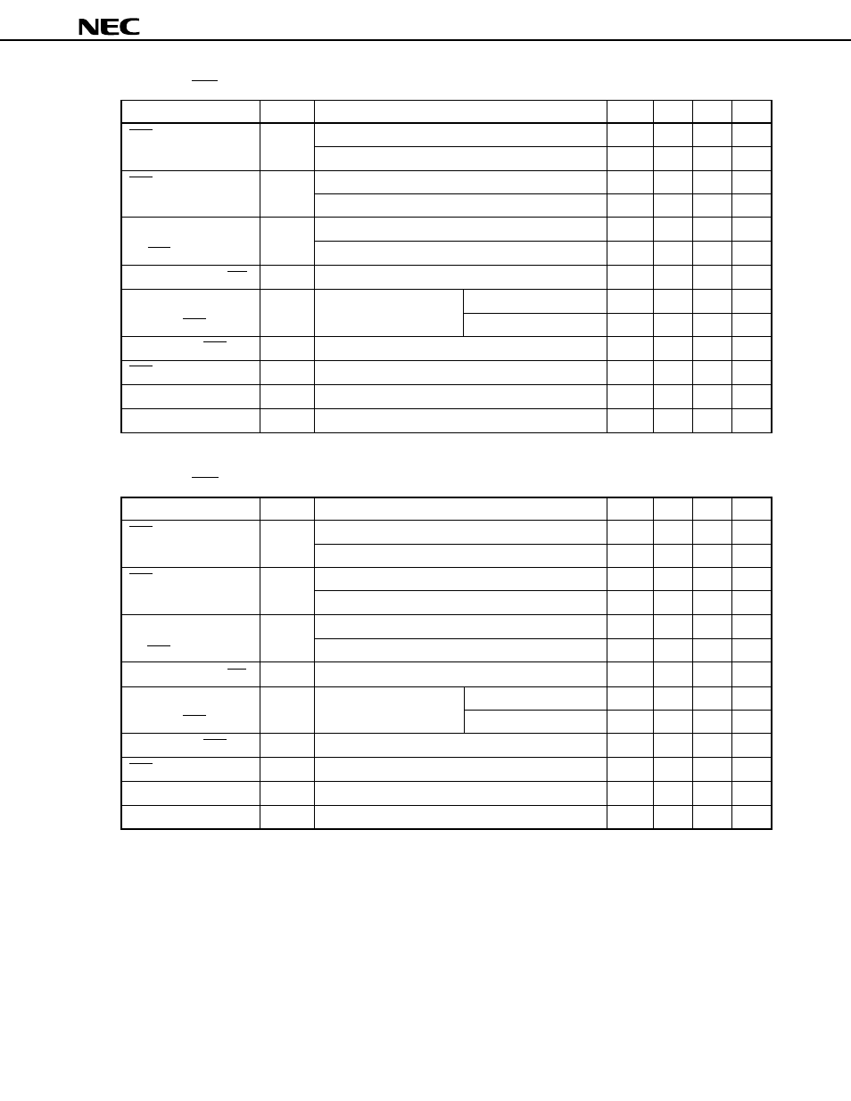
SBI mode (SCK...Internal clock output (master)): (T
A
= –40 to +85˚C, V
DD
= 1.8 to 5.5 V)
Parameter
Symbol
Test Conditions
MIN.
TYP.
MAX.
Unit
SCK cycle time
t
KCY3
V
DD
= 2.7 to 5.5 V
1300
ns
V
DD
= 1.8 to 5.5 V
3800
ns
SCK high-/low-level
t
KL3
,
t
KH3
V
DD
= 2.7 to 5.5 V
t
KCY3
/2–50
ns
width
V
DD
= 1.8 to 5.5 V
t
KCY3
/2–150
ns
SB0, 1 setup time
t
SIK3
V
DD
= 2.7 to 5.5 V
150
ns
(to SCK
↑
)
V
DD
= 1.8 to 5.5 V
500
ns
SB0, 1 hold time (from SCK
↑
)
t
KSI3
t
KCY3
/2
ns
SB0, 1 output delay
t
KSO3
R
L
= 1 k
Ω
,
V
DD
= 2.7 to 5.5 V
0
250
ns
time from SCK
↓
C
L
= 100 pF
Note
V
DD
= 1.8 to 5.5 V
0
1000
ns
SB0, 1
↓
from SCK
↑
t
KSB
t
KCY3
ns
SCK
↓
from SB0, 1
↓
t
SBK
t
KCY3
ns
SB0, 1 low-level width
t
SBL
t
KCY3
ns
SB0, 1 high-level width
t
SBH
t
KCY3
ns
Note
R
L
and C
L
are the load resistance and load capacitance of the SB0 and SB1 output lines, respectively.
SBI mode (SCK...External clock input (slave)): (T
A
= –40 to +85˚C, V
DD
= 1.8 to 5.5 V)
Parameter
Symbol
Test Conditions
MIN.
TYP.
MAX.
Unit
SCK cycle time
t
KCY4
V
DD
= 2.7 to 5.5 V
800
ns
V
DD
= 1.8 to 5.5 V
3200
ns
SCK high-/low-level
t
KL4
,
t
KH4
V
DD
= 2.7 to 5.5 V
400
ns
width
V
DD
= 1.8 to 5.5 V
1600
ns
SB0, 1 setup time
t
SIK4
V
DD
= 2.7 to 5.5 V
100
ns
(to SCK
↑
)
V
DD
= 1.8 to 5.5 V
150
ns
SB0, 1 hold time (from SCK
↑
)
t
KSI4
t
KCY4
/2
ns
SB0, 1 output delay
t
KSO4
R
L
= 1 k
Ω
,
V
DD
= 2.7 to 5.5 V
0
300
ns
time from SCK
↓
C
L
= 100 pF
Note
V
DD
= 1.8 to 5.5 V
0
1000
ns
SB0, 1
↓
from SCK
↑
t
KSB
t
KCY4
ns
SCK
↓
from SB0, 1
↓
t
SBK
t
KCY4
ns
SB0, 1 low-level width
t
SBL
t
KCY4
ns
SB0, 1 high-level width
t
SBH
t
KCY4
ns
Note
R
L
and C
L
are the load resistance and load capacitance of the SB0 and SB1 output lines, respectively.