One-time prom (program memory) write and verify, 1 operation modes for program memory write/verify – NEC uPD75P3116 User Manual
Page 28
µ
PD75P3116
28
Data Sheet U11369EJ3V0DS
8. ONE-TIME PROM (PROGRAM MEMORY) WRITE AND VERIFY
The program memory contained in the
µPD75P3116 is a 16384 × 8-bit one-time PROM that can be electrically written
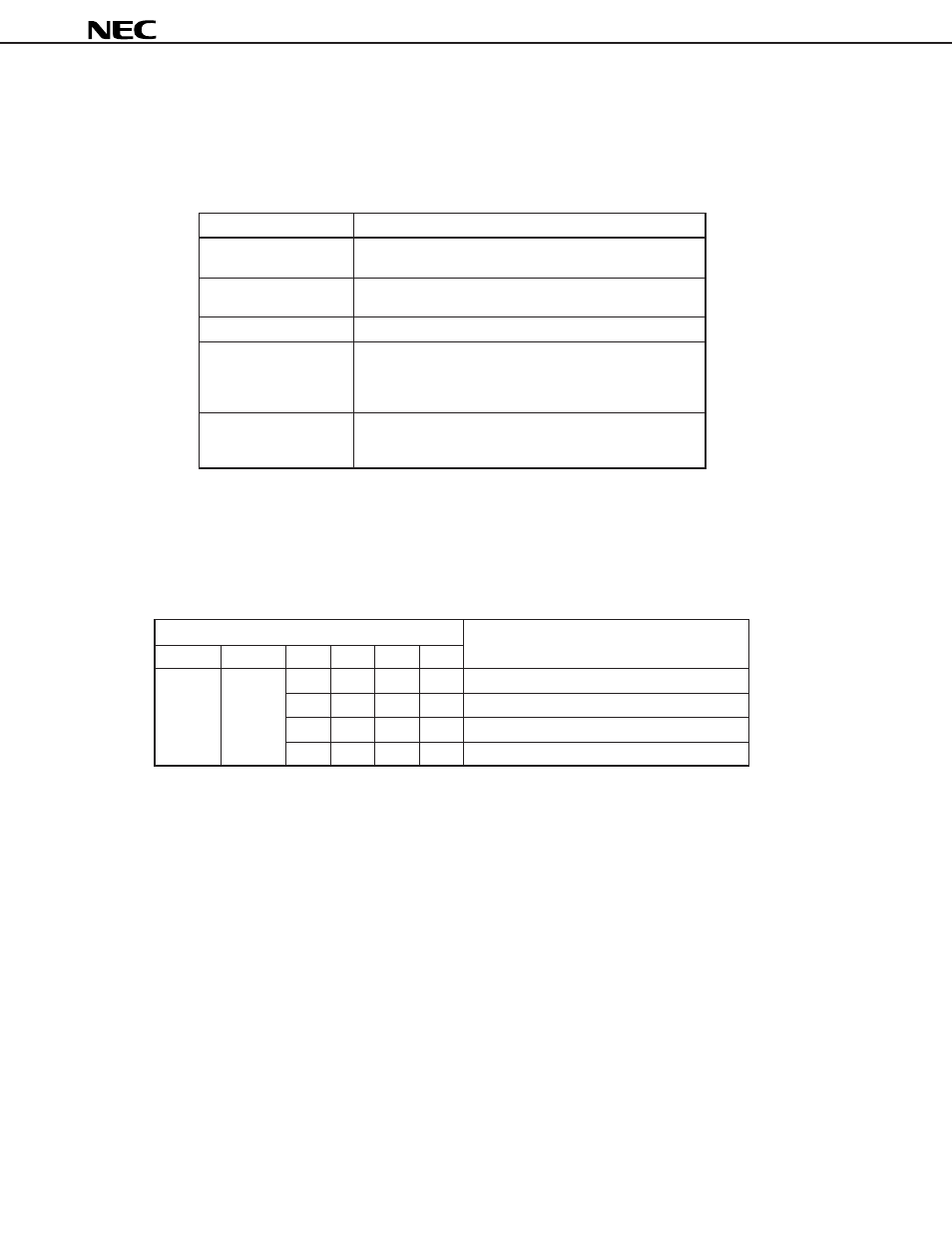
one time only. The pins listed in the table below are used for this PROM’s write/verify operations. Clock input from the
X1 pin is used instead of address input as a method for updating addresses.
Pin
Function
V
PP
Pin where program voltage is applied during program memory
write/verify (usually V
DD
potential)
X1, X2
Clock input pins for address updating during program memory
write/verify. Input the X1 pin’s inverted signal to the X2 pin.
MD0 to MD3
Operation mode selection pin for program memory write/verify
D0/P60 to D3/P63
8-bit data I/O pins for program memory write/verify
(lower 4 bits)
D4/P50 to D7/P53
(higher 4 bits)
V
DD
Pin where power supply voltage is applied. Apply 1.8 to 5.5 V
in normal operation mode and +6 V for program memory write/
verify.
Caution
Pins not used for program memory write/verify should be connected to Vss.
8.1 Operation Modes for Program Memory Write/Verify
When +6 V is applied to the V
DD
pin and +12.5 V to the V
PP
pin, the
µPD75P3116 enters the program memory write/
verify mode. The following operation modes can be specified by setting pins MD0 to MD3 as shown below.
Operation Mode Specification
Operation Mode
V
PP
V
DD
MD0
MD1
MD2
MD3
+12.5 V
+6 V
H
L
H
L
Zero-clear program memory address
L
H
H
H
Write mode
L
L
H
H
Verify mode
H
×
H
H
Program inhibit mode
×: L or H