Application information, Ic card interf ace td a8002c, Fig.16 application diagram – Philips TDA8002C User Manual
Page 22
1999
Oct
12
22
Philips Semiconductors
Product specification
IC card interf
ace
TD
A8002C
This text is here in white to force landscape pages to be rotated correctly when browsing through the pdf in the Acrobat reader.This text is here in
_
white to force landscape pages to be rotated correctly when browsing through the pdf in the Acrobat reader.This text is here inThis text is here in
white to force landscape pages to be rotated correctly when browsing through the pdf in the Acrobat reader. white to force landscape pages to be ...
APPLICA
TION INFORMA
TION
u
ll pagewidth
FCE195
C8
10
µ
F
C4
(3)
100 nF
C3
(2)
100
nF
C5
(4)
470 nF
C7
100 nF
C6
(5)
470 nF
80C51
P1-0
P1-1
P1-2
P1-3
P1-4
P1-5
P1-6
P1-7
RST
P3-0
P3-1
P3-2
P3-3
P3-4
P3-5
P3-6
P3-7
XTAL2
XTAL1
VSS
VCC
P0-0
P0-1
P0-2
P0-3
P0-4
P0-5
P0-6
P0-7
EA
ALE
PSEN
P2-7
P2-6
P2-5
P2-4
P2-3
P2-2
P2-1
P2-0
XTAL1
XTAL2
I/OUC
AUX1UC
CS
ALARM
CLKSEL
CLKDIV1
CLKDIV2
STROBE
CLKOUT
DGND1
AGND
S2
IC2
IC1
MODE
OFF
RSTIN
CMDVCC
RST
CLK
VCC
AUX1
PRES
I/O
VUP
S1
VDDA
VDD
1
2
3
4
5
6
7
8
9
10
11
12
13
28
27
26
25
24
23
22
21
20
19
28
27
26
25
24
23
22
21
30
29
38
37
36
35
34
33
32
31
40
39
18
17
16
15
14
1
2
3
4
5
15
6
7
8
9
10
16
17
18
19
20
11
12
13
14
TDA8002CT/C
CV/TV
C5I
C6I
C7I
C8I
C1I
C2I
C3I
C4I
C4
C3
C2
C1
C8
C7
C6
C5
(1)
K1
K2
33 pF
33 pF
14.745
MHz
VDD
C2
10
µ
F
C1
100 nF
VDD
J1 1
3.3 V or 5 V
J1 2
ground
CARD READ
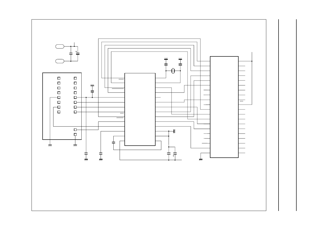
Fig.16 Application diagram.
TDA8002C should be placed as close as possible to the card reader.
(1) Contact normally open.
(2) C3 close to pin V
CC
of TDA8002C.
(3) C4 close to C1 contact of card reader.
(4) C5 close to VUP pin of TDA8002C.
(5) C6 as close as possible to pins S1 and S2.
CLK line may be shielded with respect to other lines.
Decoupling capacitors C7 and C8 may be placed as close as possible to pin V
DDA
.
A good ground plane is recommended.