Serial interface description – PMC-Sierra Pm25LV512 User Manual
Page 5
5
Programmable Microelectronics Corp.
Issue Date: February, 2004, Rev: 1.4
PMC
Pm25LV512/010
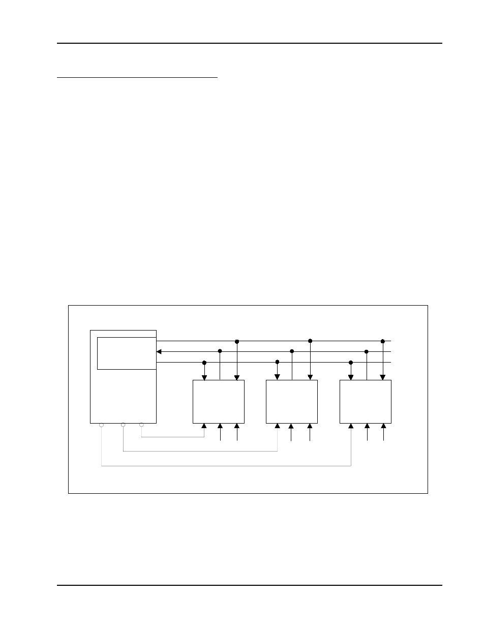
Pm25LV512/010 can be driven by a microcontroller on the SPI bus as shown in Figure 1. The serial communication
term definitions are in the following section.
MASTER: The device that generates the serial clock.
SLAVE: Because the Serial Clock pin (SCK) is always an input, the Pm25LV512/010 always operates as a slave.
TRANSMITTER/RECEIVER: The Pm25LV512/010 has separate pins designated for data transmission (SO) and
reception (Sl).
MSB: The Most Significant Bit (MSB) is the first bit transmitted and received.
SERIAL OP-CODE: After the device is selected with CE# going low, the first byte will be received. This byte
contains the op-code that defines the operations to be performed.
INVALID OP-CODE: If an invalid op-code is received, no data will be shifted into the Pm25LV512/010, and the serial
output pin (SO) will remain in a high impedance state until the falling edge of CE# is detected again. This will
reinitialize the serial communication.
SERIAL INTERFACE DESCRIPTION
SPI Interface with
(0, 0) or (1, 1)
S D O
SDI
S C K
S C K
S O
SI
Bus Master
C S 3
C S 2 C S 1
C E #
W P # H O L D #
H O L D #
H O L D #
SPI Memory
Device
SPI Memory
Device
SPI Memory
Device
Note: 1. The Write Protect (WP#) and Hold (HOLD#) si gnals should be driven, Hi gh or Low as appropriate.
S C K S O
SI
S C K
S O
SI
C E #
W P #
C E #
W P #
Figure 1. Bus Master and SPI Memory Devices