Philips SA7016 User Manual
Page 6
Philips Semiconductors
Product specification
SA7016
1.3GHz low voltage fractional-N synthesizer
1999 Nov 04
6
SYMBOL
UNIT
MAX.
TYP.
MIN.
CONDITIONS
PARAMETER
Phase noise (R
SET
= 7.5 k
Ω
, CP=00)
L
Synthesizer’s contribution to close-in phase noise
of 900 MHz RF signal at 1 kHz offset.
GSM
f
REF
= 13MHz, TCXO,
f
COMP
= 1MHz
indicative, not tested
–
–90
–
dBc/Hz
L
(f)
Synthesizer’s contribution to close-in phase noise
of 800 MHz RF signal at 1 kHz offset.
TDMA
f
REF
= 19.44MHz, TCXO,
f
COMP
= 240kHz
indicative, not tested
–
–85
–
dBc/Hz
Interface logic input signal levels; pins 13, 14, 15, 16
V
IH
HIGH level input voltage
0.7*V
DD
–
V
DD
+0.3
V
V
IL
LOW level input voltage
–0.3
–
0.3*V
DD
V
I
LEAK
Input leakage current
logic 1 or logic 0
–0.5
–
+0.5
µ
A
Lock detect output signal (in push/pull mode); pin 1
V
OL
LOW level output voltage
I
sink
=2mA
–
–
0.4
V
V
OH
HIGH level output voltage
I
source
=–2mA
V
DD
–0.4
–
–
V
NOTES:
1. I
SET =
V
SET
R
SET
bias current for charge pumps.
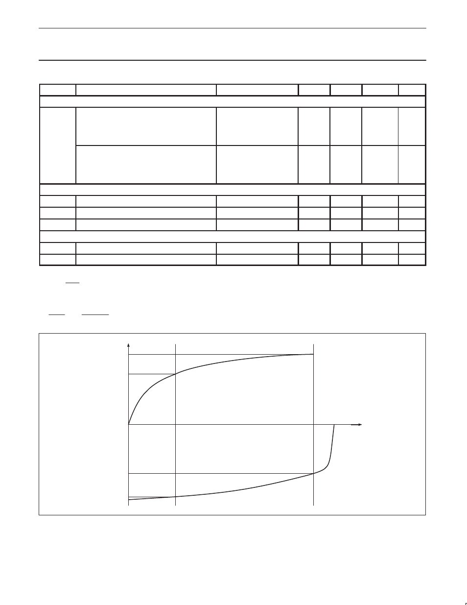
2. The relative output current variation is defined as:
D
I
OUT
I
OUT
+
2
.
(I
2
–I
1
)
I(I
2
)
I
1
)I
; with V
1
+
0.7V, V
2
+
V
DDCP
–0.8V (See Figure 3.)
I
2
I
1
I
2
I
1
V
1
V
2
CURRENT
V
PH
SR00602
I
ZOUT
Figure 3.
Relative Output Current Variation