Pinning – Philips SA7016 User Manual
Page 3
Philips Semiconductors
Product specification
SA7016
1.3GHz low voltage fractional-N synthesizer
1999 Nov 04
3
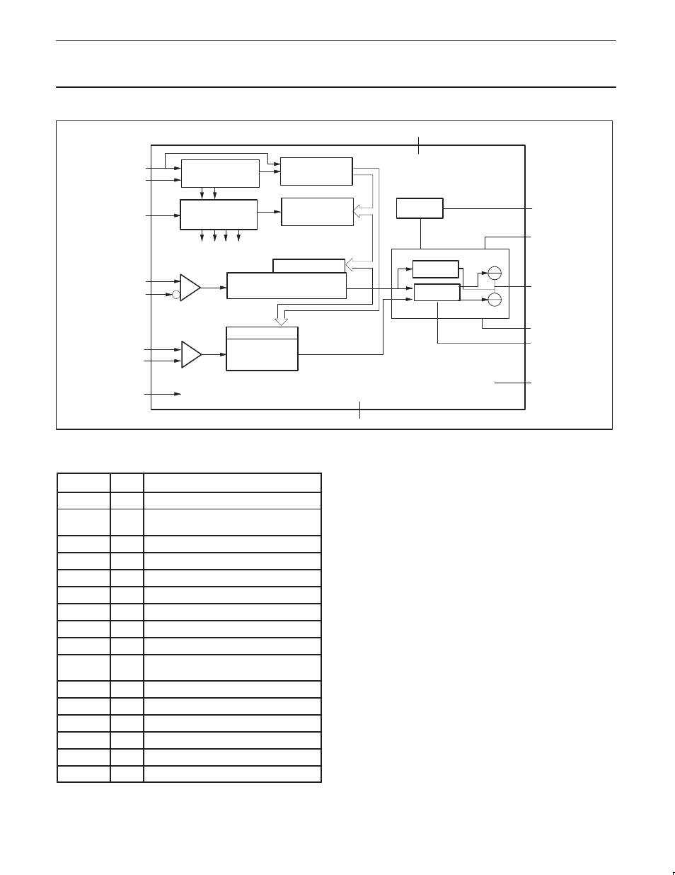
SR01506
CLOCK
DATA
STROBE
RFin+
RFin–
REF
in+
REF
in–
TEST
LOAD SIGNALS
ADDRESS DECODER
2–BIT SHIFT
REGISTER
22–BIT SHIFT
REGISTER
CONTROL
LATCH
LATCH
MAIN DIVIDER
REFERENCE
DIVIDER
LATCH
AMP
11
12
6
5
15
14
13
2
PHASE
DETECTOR
COMP
PUMP
BIAS
PUMP
CURRENT
SETTING
GND
4
7
3
GND
CP
V
DD
R
SET
V
DDCP
PHP
LOCK
10
9
8
1
PON
16
Figure 2.
Block Diagram
PINNING
SYMBOL
PIN
DESCRIPTION
LOCK
1
Lock detect output
TEST
2
Test (should be either grounded or
connected to V
DD)
V
DD
3
Digital supply
GND
4
Digital ground
RFin+
5
RF input to main divider
RFin–
6
RF input to main divider
GND
CP
7
Charge pump ground
PHP
8
Main normal chargepump
V
DDCP
9
Charge pump supply voltage
R
SET
10
External resistor from this pin to ground
sets the chargepump current
REFin–
11
Reference input
REFin+
12
Reference input
CLOCK
13
Programming bus clock input
DATA
14
Programming bus data input
STROBE
15
Programming bus enable input
PON
16
Power down control