Panasonic SJ-MJ88 User Manual
Page 51
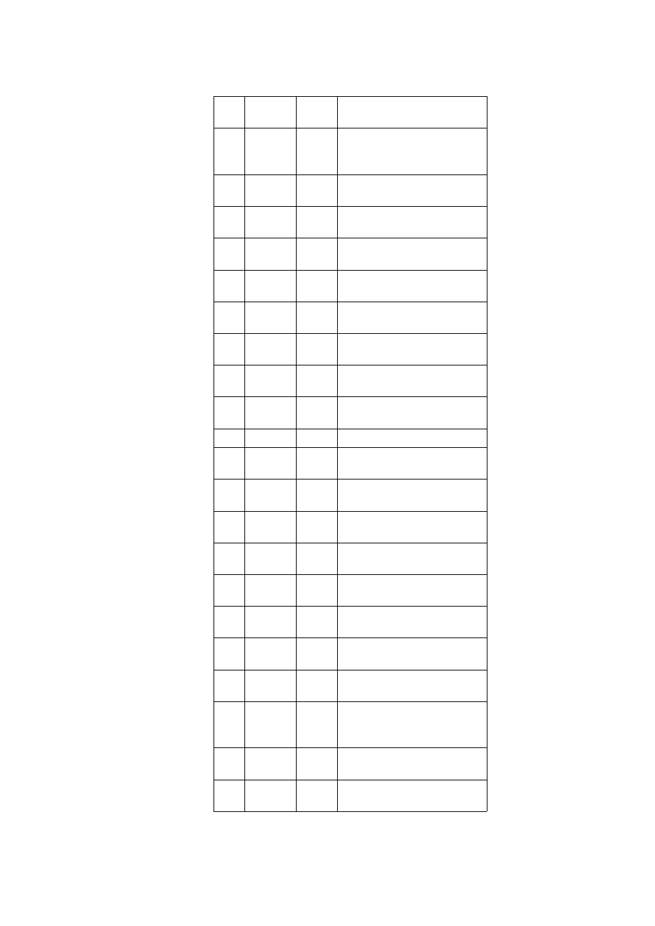
Pin
No.
Mark
I/O
Division
Function
51
BATT
CHK
LED
—
Battery check LED drive
output terminal (Not used,
open)
52
JITTER
OK
—
Process inspection output
terminal (Not used, open)
53
REG2
I
Model switching input
terminal (L:MJ88, H:MJ80)
54
REG3
I
Recharge switching input
terminal
55,
56
—
—
Not used, open
57
EEP CS
O
EEP ROM chip select
output terminal
58
EEP CK
O
EEP ROM clock output
terminal
59
EEP
DATA O
O
EEP RAM DATA output
terminal
60
EEP
DATA I
I
EEP ROM DATA input
terminal
61~64
—
—
Not used, open
65
MUTE A
O
Analog mute A output
terminal
66
MUTE B
O
Analog mute B output
terminal
67
NRF
STBY
O
RF AMP standby output
terminal
68
DRAM
CHK
I
DRAM check input terminal
69,
70
—
—
Not used, open
71
MONI
OFF
O
RF monitor control output
terminal (H:OFF, L:ON)
72
BPF
O
RF band pass filter control
output terminal (L:WIDE)
73
RF
CONT
O
RF power supply control
output terminal
74
MUTE
MODE
—
Mute mode switching input
terminal (Connected to
GND)
75
POWER
CNT
O
Power supply control
output terminal
76
ELON
I
EL display control input
terminal (L:ON)
51