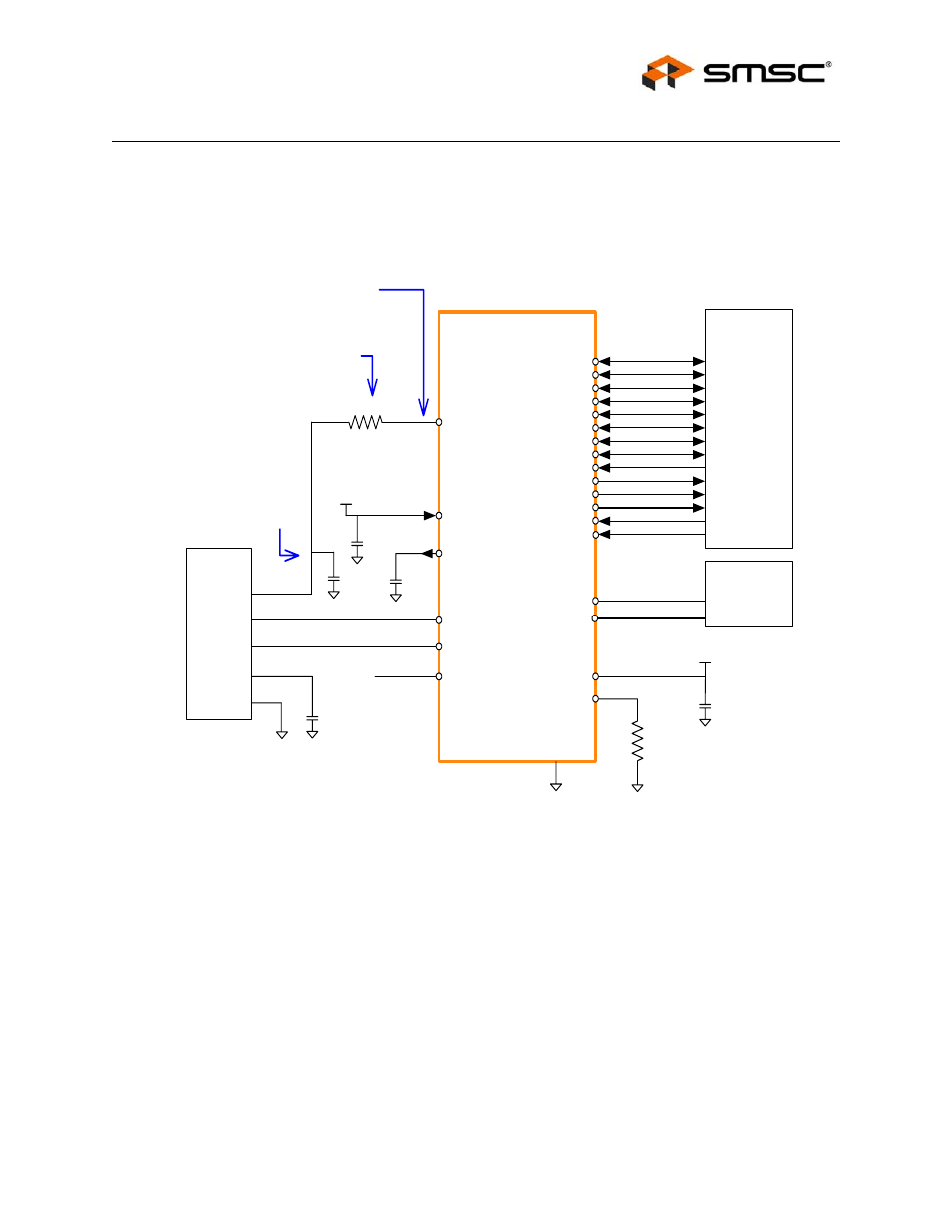
Application diagrams, Figure 3 usb3310 qfn application diagram (device), Product preview – SMSC 1.8V IO Voltage (10%) flexPWR USB3310 User Manual
Page 7: Usb331x

Hi-Speed USB Transceiver with 1.8V ULPI Interface - Multi-Frequency Reference Clock
SMSC USB3310 REV C
7
Revision 1.11 (10-31-08)
PRODUCT PREVIEW
Application Diagrams
Figure 3 USB3310 QFN Application Diagram (Device)
Link Controller
USB331X
RBIAS
DIR
NXT
STP
CLKOUT
DATA7
DATA6
DATA5
DATA4
DATA3
DATA2
DATA0
DATA1
VBAT
VDD3.3
VBUS
DM
DP
ID
RESETB
USB
Receptacle
DM
DP
DIR
NXT
STP
CLKOUT
DATA7
DATA6
DATA5
DATA4
DATA3
DATA2
DATA0
DATA1
RESETB
6
5
24
GND FLAG
2
3
VBUS
1
SHIELD
GND
4
3
2
1
C
BYP
C
VBUS
3.1-5.5V
Supply
R
VBUS
may be installed in this configuration to
assist in protecting the VBUS pin. 820 Ohms
will protect against VBUS transients up to
8.5V. 10K Ohms will protect against
transients up to 10V.
REFCLK
VDD18
21
Reference
C
OUT
C
DC_BLOCK
8.06k
Steady state voltage at the VBUS pin must not be
allowed to exceed V
VMAX
.
R
VBUS
NC
7
8
9
10
12
13
16
17
20
18
19
11
22
23
C
BYP
1.8V Supply
REFSEL[1]
14
The capacitor C
VBUS
must be
installed on this side of R
VBUS
.
Signal at REFCLK
must comply with
V
IH
and V
IL
REFSEL[0]
15
Pin Strap
Determines
REFCLK
frequency
