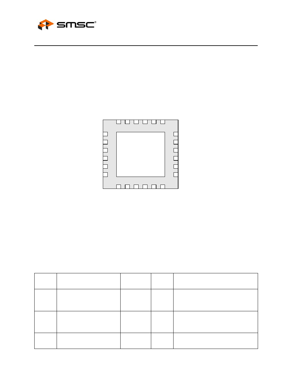
Usb3310 pin locations and descriptions, Package diagram with pin locations, Figure 2 usb3310 qfn pinout - top view – SMSC 1.8V IO Voltage (10%) flexPWR USB3310 User Manual
Page 4: Pin definitions, Table 1 usb3310 pin description, Usb3310, Pin locations and descriptions, Product preview, 24pin qfn 4x4mm
Hi-Speed USB Transceiver with 1.8V ULPI Interface - Multi-Frequency Reference Clock
Revision 1.11 (10-31-08)
4
SMSC USB3310 REV C
PRODUCT PREVIEW
USB3310
Pin Locations and Descriptions
Package Diagram with Pin Locations
The pinout below is viewed from the top of the package.
Pin Definitions
The following table details the pin definitions for the figure above.
Figure 2 USB3310 QFN Pinout - Top View
Table 1 USB3310 Pin Description
PIN
BALL
NAME
DIRECTION/
TYPE
ACTIVE
LEVEL
DESCRIPTION
1
B1
ID
Input,
Analog
N/A
ID pin of the USB cable. For non-OTG
applications this pin can be floated. For
an A-Device ID is grounded. For a B-
Device ID is floated.
2
C1
VBUS
I/O,
Analog
N/A
VBUS pin of the USB cable. This pin is
used for the Vbus comparator inputs and
for Vbus pulsing during session request
protocol.
3
C2
VBAT
Power
N/A
Regulator input. The regulator supply can
be from 5.5V to 3.1V.
DAT
A
7
VBUS
ID
VDD3.3
DM
DP
NXT
DI
R
ST
P
DAT
A
3
DATA1
REFSEL[1]
DATA2
REFSEL[0]
VBAT
V
DD1
.8
CL
KOUT
DAT
A
5
DAT
A
6
DAT
A
4
1
2
3
4
5
6
7
8
9
10
11
12
18
17
16
15
14
13
24
23
22
21
20
19
24Pin QFN
4x4mm
RE
SET
B
DATA0
RB
IA
S
RE
FCL
K