Sclk, Sdio, Sclk sdio – Silicon Laboratories SI4734/35-B20 User Manual
Page 8
S i 4 7 3 4 / 3 5 - B 2 0
8
Rev. 1.0
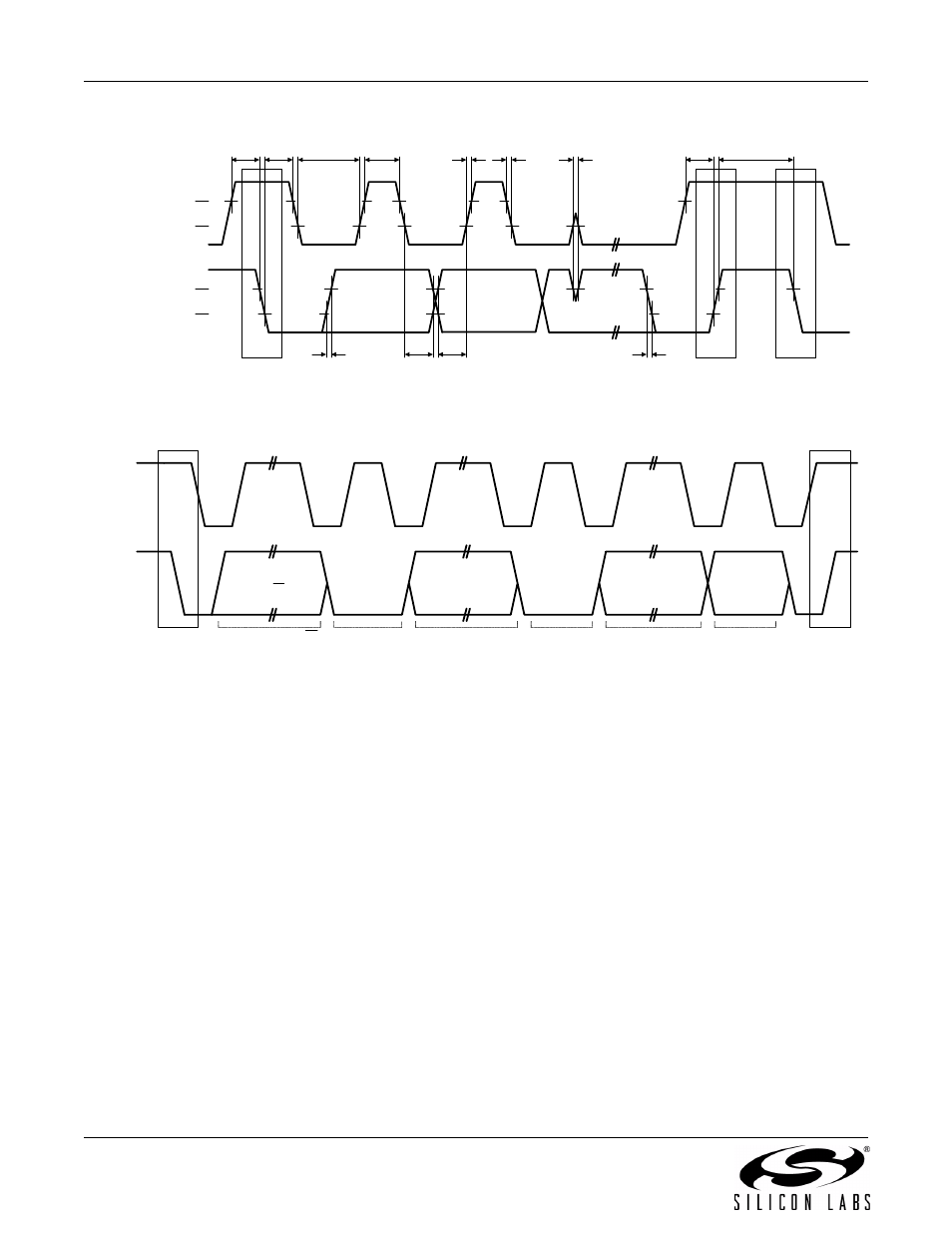
Figure 2. 2-Wire Control Interface Read and Write Timing Parameters
Figure 3. 2-Wire Control Interface Read and Write Timing Diagram
SCLK
70%
30%
SDIO
70%
30%
START
START
STOP
t
f:IN
t
r:IN
t
LOW
t
HIGH
t
HD:STA
t
SU:STA
t
SU:STO
t
SP
t
BUF
t
SU:DAT
t
r:IN
t
HD:DAT
t
f:IN,
t
f:OUT
SCLK
SDIO
START
STOP
ADDRESS + R/W
ACK
DATA
ACK
DATA
ACK
A6-A0,
R/W
D7-D0
D7-D0