Pin descriptions: si4734/35-gm, Gnd pad – Silicon Laboratories SI4734/35-B20 User Manual
Page 30
S i 4 7 3 4 / 3 5 - B 2 0
30
Rev. 1.0
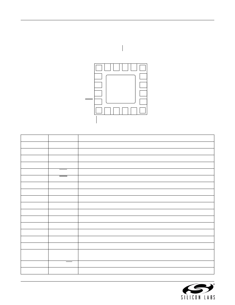
6. Pin Descriptions: Si4734/35-GM
Pin Number(s)
Name
Description
1, 20
NC
No connect. Leave floating.
2
FMI
FM RF inputs.
3
RFGND
RF ground. Connect to ground plane on PCB.
4
AMI
AM/SW/LW RF input.
5
RST
Device reset (active low) input.
6
SEN
Serial enable input (active low).
7
SCLK
Serial clock input.
8
SDIO
Serial data input/output.
9
RCLK
External reference oscillator input.
10
V
IO
I/O supply voltage.
11
V
DD
Supply voltage. May be connected directly to battery.
12, GND PAD
GND
Ground. Connect to ground plane on PCB.
13
ROUT
Right audio line output in analog output mode.
14
LOUT
Left audio line output in analog output mode.
15
DOUT
Digital output data in digital output mode.
16
DFS
Digital frame synchronization input in digital output mode.
17
GPO3/DCLK
General purpose output, crystal oscillator, or digital bit synchronous clock input
in digital output mode.
18
GPO2/INT
General purpose output or interrupt pin.
19
GPO1
General purpose output.
GND
PAD
1
2
3
17
18
19
20
11
12
13
14
6
7
8
9
4
5
16
10
15
GP
O2/
IN
T
VI
O
DOUT
LOUT
ROUT
GND
RST
NC
AMI
RC
LK
SD
IO
VDD
FMI
RFGND
GP
O3/
DCLK
NC
GP
O1
DF
S
SC
LK
SE
N