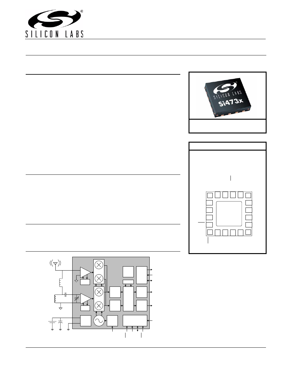
Silicon Laboratories SI4734/35-B20 User Manual
A m / f m / s w / lw r, A d i o, Features applications description

Rev. 1.0 4/08
Copyright © 2008 by Silicon Laboratories
Si4734/35-B20
S i 4 7 3 4 / 3 5 - B 2 0
B
R O A D C A S T
A M / F M / S W / LW R
A D I O
R
E C E I V E R
Features
Applications
Description
The Si4734/35 is the first digital CMOS AM/FM/SW/LW radio receiver IC that
integrates the complete tuner function from antenna input to audio output.
Functional Block Diagram
Worldwide FM band support
(64–108 MHz)
Worldwide AM band support
(520–1710 kHz)
SW band support (2.3–21.85 MHz)
LW band support (153–279 KHz)
Excellent real-world performance
Freq synthesizer with integrated VCO
Automatic frequency control (AFC)
Automatic gain control (AGC)
Integrated LDO regulator
Digital FM stereo decoder
Programmable de-emphasis
Adaptive noise suppression
AM/FM/SW/LW digital tuning
No manual alignment necessary
Adjustable channel filters
EN55020 complaint
Programmable reference clock
Digital volume control
Adjustable soft mute control
RDS/RBDS processor (Si4735 only)
Optional digital audio out (Si4735 only)
2-wire and 3-wire control interface
2.7 to 5.5 V supply voltage
Wide range of ferrite loop sticks and air
loop antennas supported
3 x 3 x 0.55 mm 20-pin QFN package
z
Pb-free/RoHS compliant
Table and portable radios
Stereos
Mini/micro systems
CD/DVD players
Portable media players
Boom boxes
Cellular handsets
Modules
Clock radios
Mini HiFi
Entertainment systems
ADC
ADC
Si4734/35
DSP
DAC
DAC
FMI
FM / SW
ANT
VIO
1.5-3.6V
SC
LK
SDIO
CONTROL
INTERFACE
SEN
RS
T
ROUT
LOUT
LDO
VDD
GND
2.7 - 5.5 V
RDS
(Si4735)
AM / LW
ANT
RFGND
AMI
LNA
LNA
LOW-IF
DIGITAL
AUDIO
(Si4735)
DOUT
DFS
GPO/DCLK
AGC
AGC
AFC
RC
LK
Patents pending
Notes:
1. To ensure proper operation and
receiver performance, follow the
guidelines in “AN383: Antenna
Selection and Universal Layout
Guide.” Silicon Laboratories will
evaluate schematics and layouts for
qualified customers.
2. Place Si4734/35 as close as
possible to antenna jack and keep
the FMI and AMI traces as short as
possible.
Ordering Information:
See page 31.
Pin Assignments
GND
PAD
1
2
3
17
18
19
20
11
12
13
14
6
7
8
9
4
5
16
10
15
GP
O
2/IN
T
VIO
DOUT
LOUT
ROUT
GND
RST
NC
AMI
RC
LK
SDI
O
VDD
FMI
RFGND
GP
O
3/D
CL
K
NC
GP
O
1
DF
S
SC
LK
SE
N
Si4734/35-GM
(Top View)
Document Outline
- Features
- Applications
- Description
- Functional Block Diagram
- 1. Electrical Specifications
- Table 1. Recommended Operating Conditions
- Table 2. Absolute Maximum Ratings1,2
- Table 3. DC Characteristics
- Table 4. Reset Timing Characteristics1,2,3
- Figure 1. Reset Timing Parameters for Busmode Select
- Table 5. 2-Wire Control Interface Characteristics1,2,3
- Figure 2. 2-Wire Control Interface Read and Write Timing Parameters
- Figure 3. 2-Wire Control Interface Read and Write Timing Diagram
- Table 6. 3-Wire Control Interface Characteristics
- Figure 4. 3-Wire Control Interface Write Timing Parameters
- Figure 5. 3-Wire Control Interface Read Timing Parameters
- Table 7. SPI Control Interface Characteristics
- Figure 6. SPI Control Interface Write Timing Parameters
- Figure 7. SPI Control Interface Read Timing Parameters
- Table 8. Digital Audio Interface Characteristics
- Figure 8. Digital Audio Interface Timing Parameters, I2S Mode
- Table 9. FM Receiver Characteristics1,2
- Table 10. 64–75.9 MHz Input Frequency FM Receiver Characteristics1
- Table 11. AM/SW/LW Receiver Characteristics1
- Table 12. Reference Clock and Crystal Characteristics
- 2. Typical Application Schematic
- 3. Bill of Materials
- 4. Functional Description
- 4.1. Overview
- 4.2. Operating Modes
- 4.3. FM Receiver
- 4.4. AM Receiver
- 4.5. SW Receiver
- 4.6. LW Receiver
- 4.7. Digital Audio Interface (Si4735 Only)
- 4.8. Stereo Audio Processing
- 4.9. De-emphasis
- 4.10. Stereo DAC
- 4.11. Soft Mute
- 4.12. RDS/RBDS Processor (Si4735 Only)
- 4.13. Tuning
- 4.14. Seek
- 4.15. Reference Clock
- 4.16. Control Interface
- 4.17. GPO Outputs
- 4.18. Firmware Upgrades
- 4.19. Reset, Power Up, and Power Down
- 4.20. Programming with Commands
- 5. Commands and Properties
- 6. Pin Descriptions: Si4734/35-GM
- 7. Ordering Guide
- 8. Package Markings (Top Marks)
- 9. Package Outline: Si4734/35 QFN
- 10. PCB Land Pattern: Si4734/35 QFN
- 11. Additional Reference Resources
- Document Change List
- Contact Information
