Typical application schematic – Silicon Laboratories SI4734/35-B20 User Manual
Page 17
S i 4 7 3 4 / 3 5 - B 2 0
Rev. 1.0
17
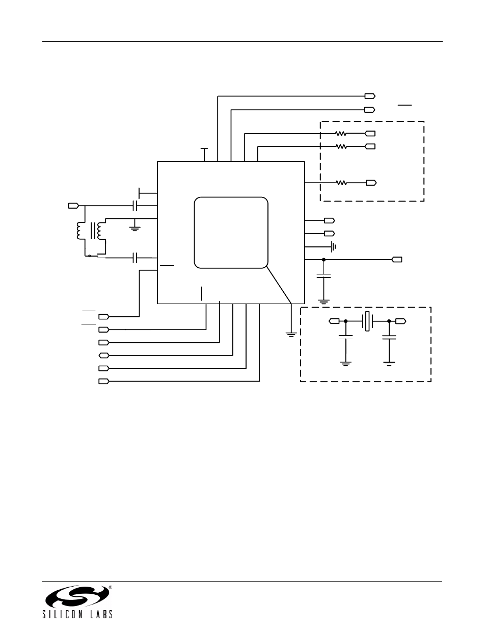
2. Typical Application Schematic
Notes:
1. Place C1 close to V
DD
pin.
2. All grounds connect directly to GND plane on PCB.
3. Pins 1 and 20 are no connects, leave floating.
4. To ensure proper operation and receiver performance, follow the guidelines in “AN383: Antenna Selection and Universal
Layout Guide.” Silicon Laboratories will evaluate schematics and layouts for qualified customers.
5. Pin 2 connects to the FM antenna interface, and pin 4 connects to the AM antenna interface.
6. RFGND should be locally isolated from GND.
7. Place Si4734/35 as close as possible to antenna jack and keep the FMI and AMI traces as short as possible.
8. See “AN382: Si4734/35 Designer’s Guide” for further recommendations.
20
19
18
17
16
U1
Si4734/35-GM
NC
FMI
RFGND
AMI
RST
DOUT
LOUT
ROUT
GND
VDD
NC
GPO1
GPO2
GPO3
DFS
SE
N
SC
LK
SD
IO
RC
LK
VIO
SEN
SCLK
SDIO
1
2
3
4
5
15
14
13
12
11
6
7
8
9
10
RST
RCLK
C1
VBATTERY
2.7 to 5.5 V
VIO
1.5 to 3.6 V
FMI
C2
C3
X1
RCLK
GPO3
Optional: for crystal oscillator option
C5
L1
L2
LOUT
ROUT
GPO1
GPO2/INT
DCLK
DFS
DOUT
Optional: Digital Audio Output
R1
R2
R3
C4