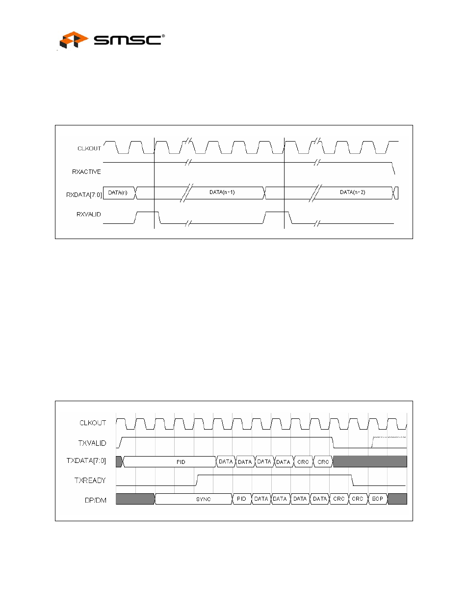
3 clock and data recovery circuit, 4 tx logic, Figure 7.3 transmit timing for a data packet – SMSC USB3280 User Manual
Page 22: Clock and data recovery circuit, Tx logic

Hi-Speed USB Device PHY with UTMI Interface
Datasheet
Revision 1.5 (11-15-07)
22
SMSC USB3280
DATASHEET
shows the relationship between CLKOUT and the receive data control signals in FS mode.
RXACTIVE "frames" a packet, transitioning only at the beginning and end of a packet. However
transitions of RXVALID may take place any time 8 bits of data are available.
also shows
how RXVALID is only asserted for one CLKOUT cycle per byte time even though the data may be
presented for the full byte time. The XCVRSELECT signal determines whether the HS or FS timing
relationship is applied to the data and control signals.
7.3
Clock and Data Recovery Circuit
This block consists of the Clock and Data Recovery Circuit and the Elasticity Buffer. The Elasticity
Buffer is used to compensate for differences between the transmitting and receiving clock domains.
The USB 2.0 specification defines a maximum clock error of ±1000ppm of drift.
7.4
TX Logic
This block receives parallel data bytes placed on the DATA bus and performs the necessary transmit
operations. These operations include parallel to serial conversion, bit stuffing and NRZI encoding.
Upon valid assertion of the proper TX control lines by the SIE and TX State Machine, the TX LOGIC
block will synchronously shift, at either the FS or HS rate, the data to the FS/HS TX block to be
transmitted on the USB cable. Data transmit timing is shown in
.
Figure 7.2 FS CLK Relationship to Receive Data and Control Signals
Figure 7.3 Transmit Timing for a Data Packet
