Input and output circuits, Video output, Cv-l105 – JAI CV-L105 User Manual
Page 6

CV-L105
5.4. Input and Output Circuits
Video outputs, timing outputs, trigger input and control inputs are found on the 68 pin LVDS
connector.
5.4.1. Video output
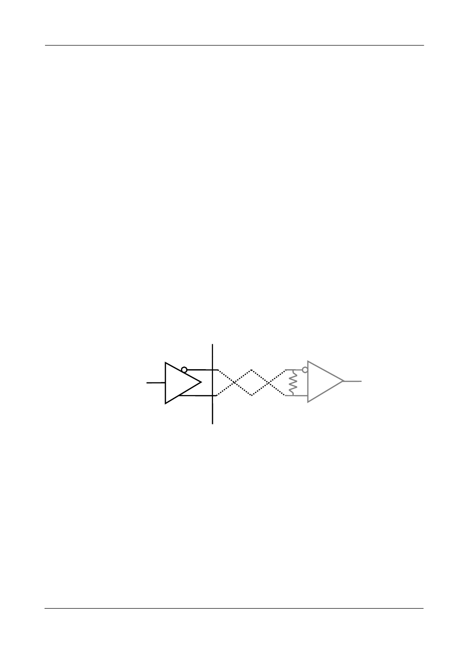
The digital EIA-644 LVDS output is constructed as follows:
Red channel video output
+RD0 to +RD7
Bits 0 to 7 positive side of the differential signal
-RD0 to –RD7
Bits 0 to 7 negative side of the differential signal
Green channel video output
+GD0 to +GD7
Bits 0 to 7 positive side of the differential signal
-GD0 to –GD7
Bits 0 to 7 negative side of the differential signal
Blue channel video output
+BD0 to +BD7
Bits 0 to 7 positive side of the differential signal
-BD0 to –BD7
Bits 0 to 7 negative side of the differential signal
Bit 0 is LSB. Bit 7 is MSB.
STROBE
This signal is used to latch the digital video into the frame grabber.
LEN
Line enable, this signal is high during the read-out of the valid digital
video.
DS90C032
100Ω
DS90C031
Image capture
Camera
Twisted pair
Fig. 5. Output driver circuit for Video, STROBE and LEN signals
- 5 -
