2 programming and verification timing for nonvol, Figure 21. timing for programming and verification, Table 18. nonvolatile memory programming and verif – Intel 8XC251SA User Manual
Page 34: Preliminary
34
PRELIMINARY
8XC251SA/SB/SP/SQ HIGH-PERFORMANCE CHMOS MICROCONTROLLER
7.2
Programming and Verification Timing for Nonvolatile Memory
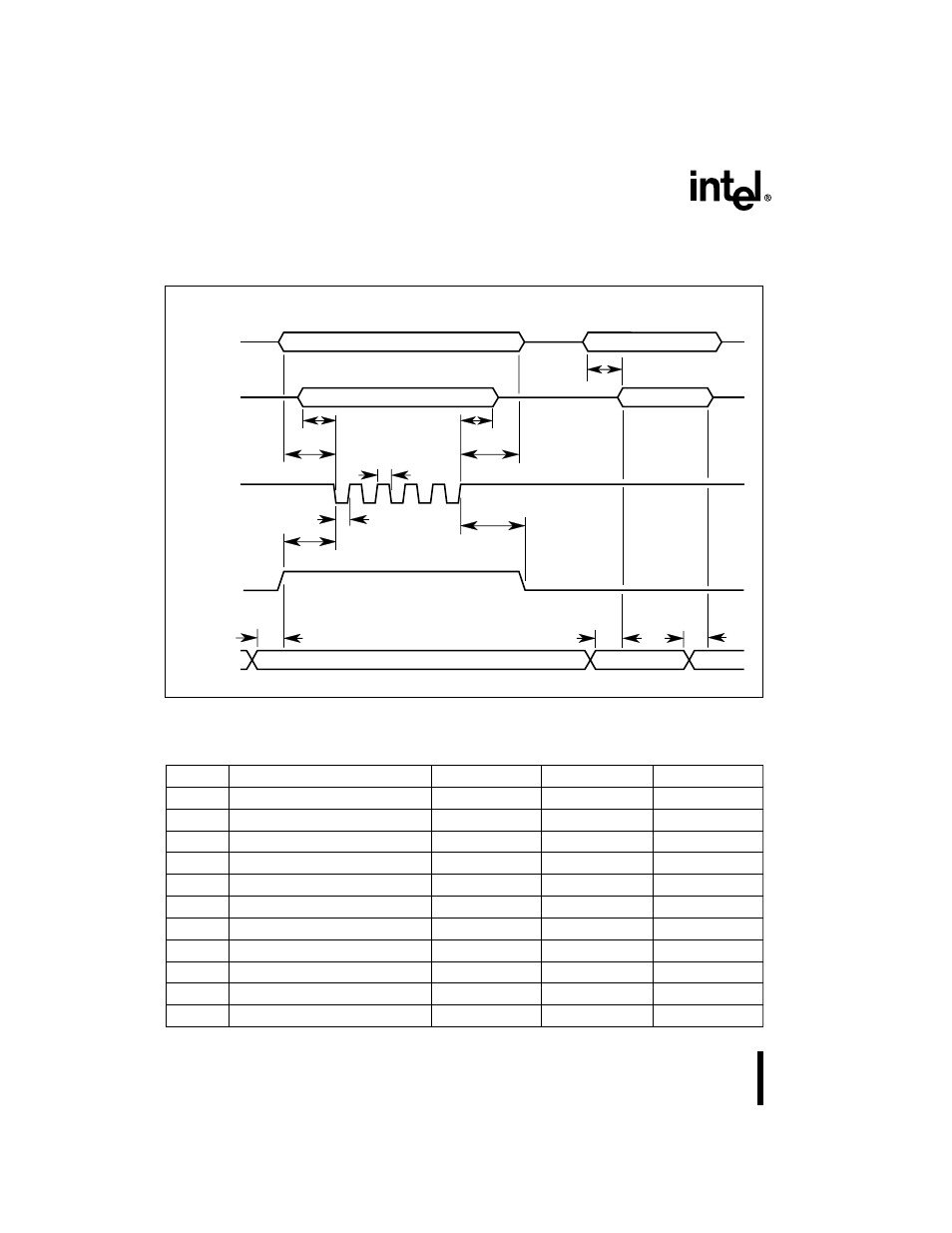
Figure 21. Timing for Programming and Verification of Nonvolatile Memory
Table 18. Nonvolatile Memory Programming and Verification Characteristics at
T
A
= 21 – 27 °C, V
CC
= 5 V, and V
SS
= 0 V
Symbol
Definition
Min
Max
Units
V
PP
Programming Supply Voltage
12.5
13.5
D.C. Volts
I
PP
Programming Supply Current
75
mA
F
OSC
Oscillator Frequency
4.0
6.0
MHz
T
AVGL
Address Setup to PROG# Low
48T
OSC
T
GHAX
Address Hold after PROG#
48T
OSC
T
DVGL
Data Setup to PROG# Low
48T
OSC
T
GHDX
Data Hold after PROG#
48T
OSC
T
EHSH
ENABLE High to V
PP
48T
OSC
T
SHGL
V
PP
Setup to PROG# Low
10
µ
s
T
GHSL
V
PP
Hold after PROG#
10
µ
s
T
GLGH
PROG# Width
90
110
µ
s
PROG#
EA#/V
PP
P1, P3
A4128-01
Address
Address (16 Bits)
P2
Data Out
Data In (8 Bits)
TAVQV
TGHDX
TGHAX
TDVGL
TAVGL
TGHGL
TGHSL
1
2
3
4
5
TGLGH
TSHGL
P0
Mode
Mode (8 Bits)
TEHSH
TELQV
TEHQZ
12.75V
Programming Cycle
Verification Cycle
5V