2 key input switch, 3 reset switch, Key input switch – FUJITSU FMB AN706 User Manual
Page 42: Reset switch
AN706-00040-2v0-E
41
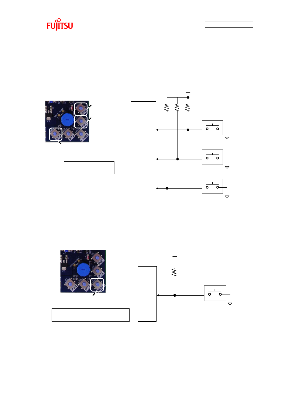
7.1.6.2 Key Input Switch
The LCD board is equipped with a power switch. The external appearance and connection
diagram of the key input switch are shown in Figure 35.
Selection Prev
Switch
Selection Next
Switch
Play/Stop Switch
Microcontroller
Pressed Down: L
Not Pressed Down: H
Pin No.52:P71
+3.3V
Selection Prev Switch (P68)
Selection Next Switch (P71)
Play/Stop Switch (P73)
Pin No.108:P68
Pin No.54:P73
Figure 35 Key Input Switch External Appearance and Connection Diagram
7.1.6.3 Reset Switch
The microcontroller board is equipped with a reset switch. The external appearance and
connection diagram of the reset switch are shown in Figure 36.
Reset Switch
Microcontroller
+3.3V
Reset Switch(Reset)
Pin No.43:INITX
Pressed Down: L (Reset Active)
Not Pressed Down: H
Reset Switch
Microcontroller
+3.3V
Reset Switch(Reset)
Pin No.43:INITX
Pressed Down: L (Reset Active)
Not Pressed Down: H
Figure 36 Reset Switch External Appearance and Connection Diagram