5 da converter, 6 switches, 1 power switch – FUJITSU FMB AN706 User Manual
Page 41: Da converter, Switches, Power switch
AN706-00040-2v0-E
40
7.1.5 DA Converter
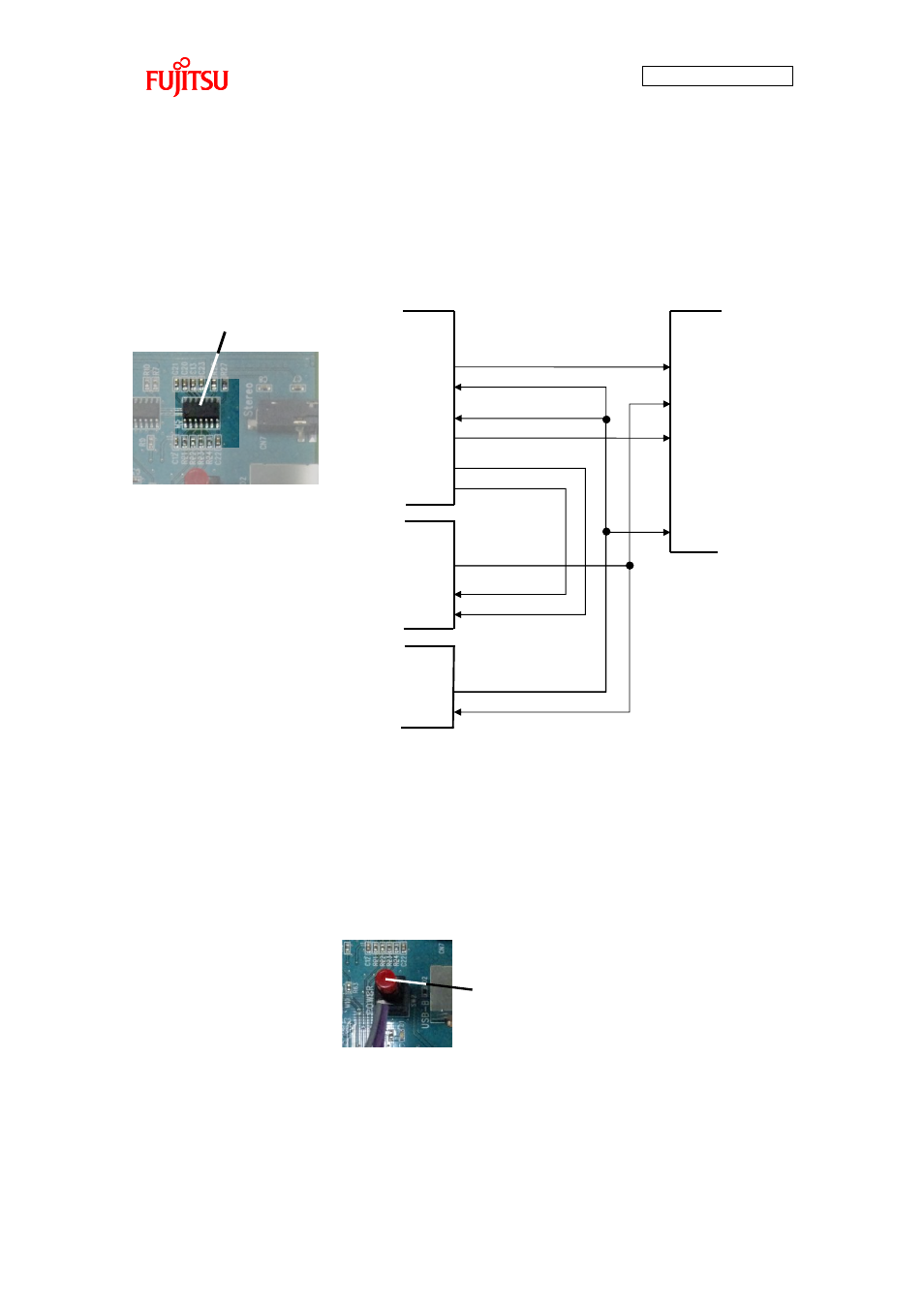
The LCD board is equipped with a DA converter for I
2
S conversion. The external
appearance and connection diagram of the DA converter are shown in Figure 33.
DA Converter
Pin No.103:SOT4_0
Pin No.111:SCK5_1
DA Converter
Pin No.2:SDIN
Pin No.3:MCLK
Pin No.4:LRCK
Pin No.5:SCLK
Clock Generator
Pin No.5:CLK
Pin No.3:S0
Pin No.104:SCK4_0
Pin No.112:SOT5_1
Pin No.113:P63
11.2896MHz
or 12.288MHz
1.4112MHz
or 1.536MHz
Binary Counter
Pin No.2:CP
Pin No.12:Q2
Pin No.6:S1
Pin No.115:P61
Microcontroller
Figure 33 DA Converter External Appearance and Connection Diagram
7.1.6 Switches
7.1.6.1 Power switch
The LCD board is equipped with a power switch. The external appearance of the power
switch is shown in Figure 34.
For power supply method, see section 3.4.
Power Switch
Figure 34 Power Switch External Appearance