Electical characteristics, Mb3788 – FUJITSU MB3788 User Manual
Page 8
MB3788
8
■
■
■
■
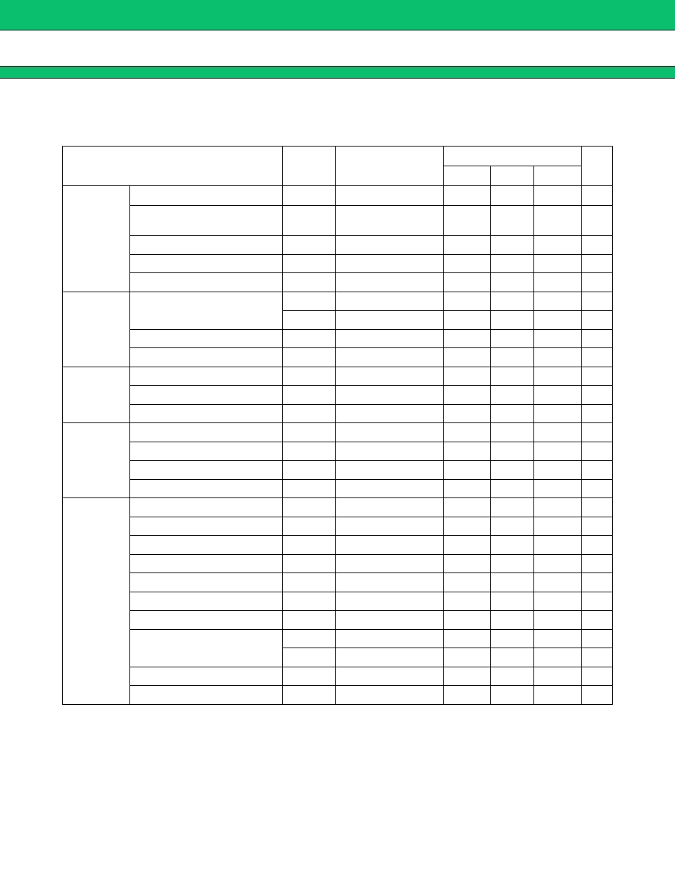
ELECTICAL CHARACTERISTICS
(Continued)
(V
CC
=6V, T
A
= +25
°
C)
Parameter
Symbol
Conditions
Value
Unit
Min
Typ
Max
Reference
voltage
Reference voltage
V
REF
I
OR
= -1 mA
2.475
2.500
2.525
V
Output voltage temperature
variation
∆
V
REF
/
V
REF
T
A
= -30
°
to +85
°
C
-2
±
0.2
2
%
Input stability
Line
V
CC
= 3.6 V to 18 V
—
2
10
mV
Load stability
Load
I
OR
= -0.1 mA to 1 mA
—
3
10
mV
Short-circuit output current
I
OS
V
REF
= 2 V
-20
-8
-3
mA
Low voltage
malfunction
fail-safe
circuit
Threshold voltage
V
tH
—
—
2.65
—
V
V
tL
—
—
2.45
—
V
Hysteresis width
V
HYS
—
80
200
—
mV
Reset voltage
V
R
—
1.5
1.9
—
V
Short-circuit
detection
comparator
Input offset voltage
V
IO
—
0.58
0.65
0.72
V
Input bias current
I
IB
V
I
= 0 V
-200
-100
—
nA
In-phase input voltage range
V
ICM
—
-0.2
—
V
CC
-1.8
V
Short-circuit
detector
Threshold voltage
V
tPC
—
0.60
0.65
0.70
V
Input standby voltage
V
STB
—
—
50
100
mV
Input latch voltage
V
I
—
—
50
100
mV
Input source current
I
Ibpc
—
-1.4
-1.0
-0.6
µ
A
Error
amplifier
Input offset voltage
V
IO
V
FB
= 1.6 V
-10
—
10
mV
Input offset current
I
IO
V
FB
= 1.6 V
-100
—
100
nA
Input bias current
I
IB
V
FB
= 1.6 V
-200
-60
—
nA
In-phase input voltage range
V
ICM
—
-0.2
—
V
CC
-1.8
V
Voltage gain
A
V
—
60
100
—
dB
Frequency bandwidth
BW
A
V
= 0 dB
—
800
—
kHz
In-phase signal rejection ratio
CMRR
—
60
80
—
dB
Maximum output voltage width
V
OM+
—
V
REF
-0.3
2.4
—
V
V
OM-
—
—
0.05
0.5
V
Output sink current
I
OM+
V
FB
= 1.6 V
—
120
—
µ
A
Output source current
I
OM-
V
FB =
1.6 V
—
-2
—
mA