Pin description – FUJITSU MB39A105 User Manual
Page 3
MB39A105
3
■
■
■
■
PIN DESCRIPTION
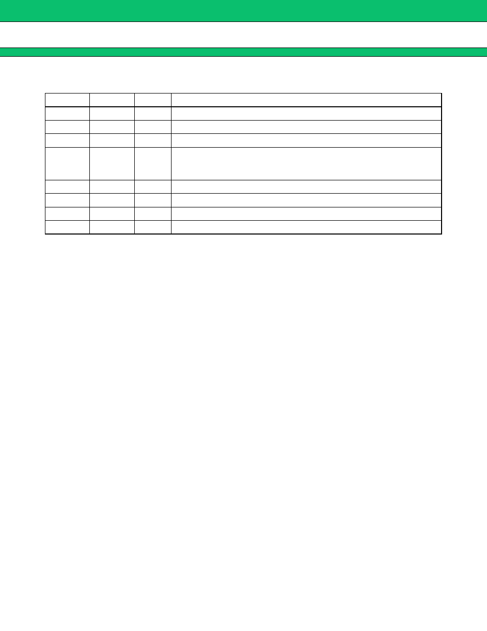
Pin No.
Symbol
I/O
Descriptions
1
−
INE
I
Error amplifiers (Error Amp) inverted input terminal
2
CSCP
Timer-latch short-circuit protection capacitor connection terminal
3
VCC
Power supply terminal
4
SCPOD
O
Open drain output terminal for short-circuit protection detection
During timer-latch short-circuit protection operation : Output “High-Z”
During normal operation : Output “L”
5
OUT
O
External Nch FET gate drive terminal
6
GND
Ground terminal
7
RT
Triangular wave oscillation frequency setting resistor connection terminal
8
FB
O
Error Amplifier (Error Amp) output terminal