Applications information, Ucsp applications information, Chip information – Rainbow Electronics MAX9519 User Manual
Page 8
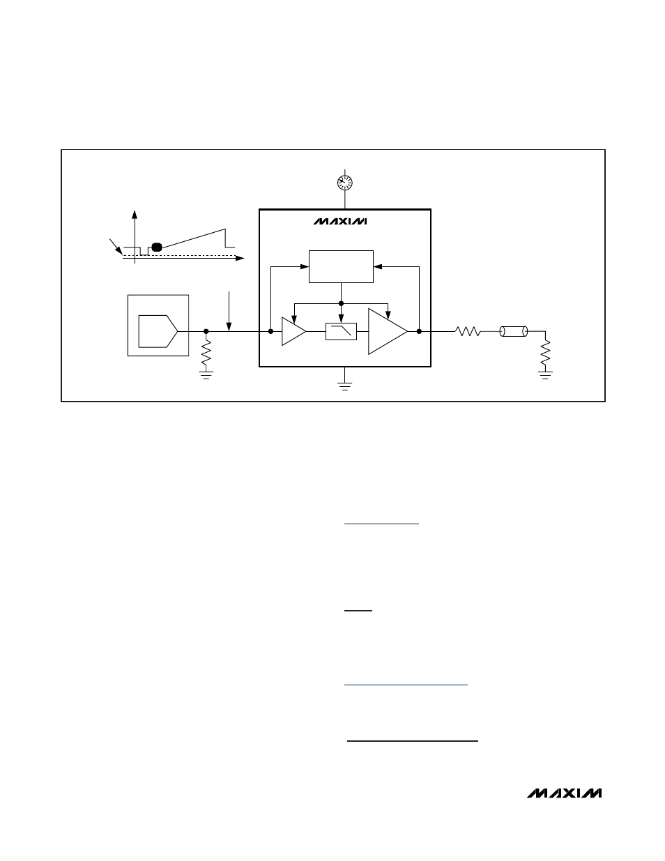
MAX9519
1mm x 1mm Video Filter Amplifier with
Automatic Shutdown and 4V/V Gain
8
_______________________________________________________________________________________
Input
The MAX9519 video input should be directly connected
to the output of the video current DAC. DC-coupling
ensures that the input signal is ground referenced such
that the sync tip of the composite video signal is within
25mV of ground. Any standard-definition video signal
can be applied to the input as long as the signal is
between ground and 0.525V when V
DD
= 2.7V.
Video Reconstruction Filter
The filter passband (±1dB) is typically 9MHz, which
makes the device suitable for standard-definition video
signals from all sources (e.g., broadcast and DVD).
Broadcast video signals are channel limited: NTSC sig-
nals have 4.2MHz bandwidth, and PAL signals have
5MHz of bandwidth. Video signals from a DVD player,
however, are not channel limited; so the bandwidth of
DVD video signals approaches the Nyquist limit of
6.75MHz. Recommendation: ITU-R BT.601-5 specifies
13.5MHz as the sampling rate for standard-definition
video. Therefore, the maximum bandwidth of the signal
is 6.75MHz. To ease the filtering requirements, most
modern video systems over sample by two times,
clocking the video current DAC at 27MHz.
Output
The MAX9519 output expects to drive a DC-coupled
load to ground. The amplifier output stage needs about
300mV of headroom from either supply rail. The device
has an internal level shift circuit that positions the sync
tip at approximately 300mV at the output.
Applications Information
Power-Supply Bypassing and Ground
The MAX9519 operates from a single-supply voltage
down to 2.7V, allowing for low-power operation. Bypass
V
DD
to GND with a 0.1µF capacitor. Place all external
components as close as possible to the device.
UCSP Applications Information
For the latest application details on UCSP construction,
dimensions, tape carrier information, PCB techniques,
bump-pad layout, and recommended reflow tempera-
ture profile, as well as the latest information on reliability
testing results, go to the Maxim’s website at
www.maxim-ic.com/ucsp
to find the Application Note
1891:
Understanding the Basics of the Wafer-Level
Chip-Scale Package (WL-CSP).
CURRENT
DAC
VIDEO ENCODER
VIDEO SIGNAL
PRESENT
A
V
= 4V/V
OUT
IN
BUFFER
LPF
AUTOMATIC
SHUTDOWN
CONTROL LOGIC
2.9mA QUIESCENT SUPPLY CURRENT NOT INCLUDING OUTPUT LOAD CURRENT
MAX9519
V
DD
+3.3V
75
Ω
75
Ω
GND
0
TO
25mV
0.5V
P-P
VIDEO
Figure 3. Full-Operation Mode
Chip Information
PROCESS: BiCMOS