Appendix b: schematic diagrams, Appendix b:schematic diagrams – Intel M570TU User Manual
Page 57
Schematic Diagrams
B - 1
B.Sch
e
m
a
tic D
iag
rams
Appendix B:Schematic Diagrams
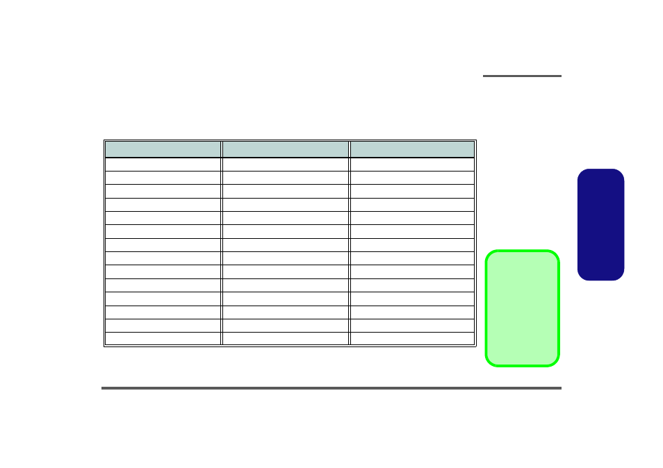
This appendix has circuit diagrams of the M570TU notebook’s PCB’s. The following table indicates where to find the
appropriate schematic diagram.
Diagram - Page
Diagram - Page
Diagram - Page
SYSTEM BLOCK DIAGRAM - Page B - 2
ICH9-M 3/4 CASE FAN - Page B - 16
Power Charger, DC IN - Page B - 30
ODD, PC BEEP, USB2.0 & eSATA - Page B - 18
Power 1.5V/ 0.75V - Page B - 32
CLOCK GENERATOR, CCD - Page B - 19
Power 1.8VS/ 1.05VS - Page B - 33
PCI-E LAN RTL8111C - Page B - 20
Power 3VS, 5VS, Power S/W - Page B - 34
CARD READER & 1394 JMB380 - Page B - 21
Power VDD3/ VDD5/ 3.3V/ 5V - Page B - 35
Crestline 4/6 POWER1 - Page B - 8
Power VCORE for Penryn CPU - Page B - 36
Cantiga 6/6 POWER2 - Page B - 10
MXM PCI-E TYPE-IV - Page B - 38
Board to board CON - Page B - 39
AZALIA CODEC ALC662 - Page B - 26
Fingerprint Board - Page B - 42
ICH9-M 2/4 PCI,USB - Page B - 15
CRT, INV, MDC, BT, PWRGD - Page B - 29
Table B - 1
Schematic
Diagrams
Version Note
The schematic dia-
grams in this chapter
are based upon ver-
sion 6-7P-M5705-005.
If your mainboard (or
other boards) are a lat-
er version, please
check with the Service
Center for updated di-
agrams (if required).