Displays, Connector pin assignment for interface – Purdy ANDpSi089C362S-4HB User Manual
Page 5

Purdy Electronics Corporation • 720 Palomar Avenue • Sunnyvale, CA 94085
1/28/08
Tel: 408.523.8216 • Fax: 408.733.1287 • [email protected]
5
www.purdyelectronics.com
Displays
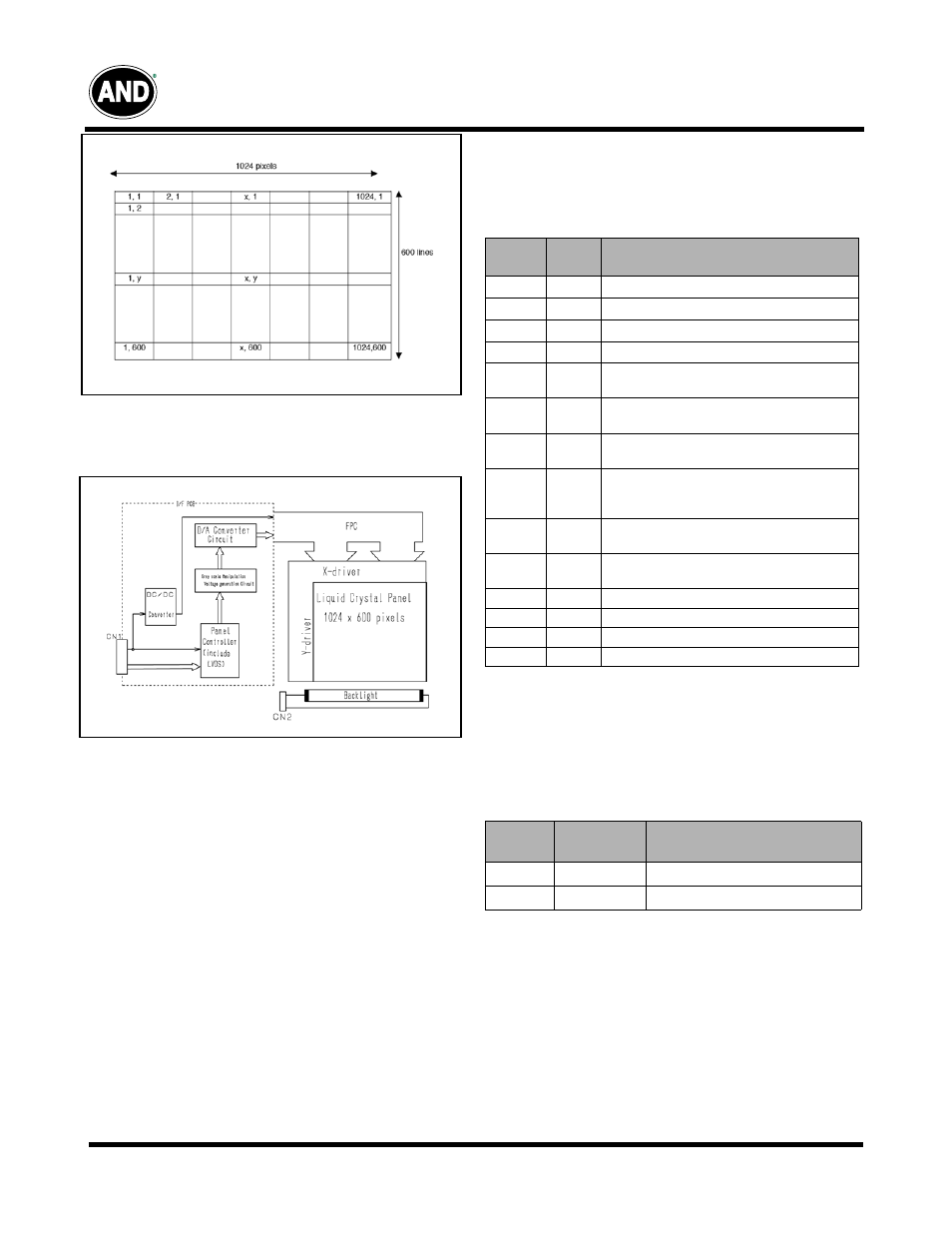
Block Diagram
Connector Pin Assignment for Interface
CN1 Input Signal
Connector: DF19L-14P-1H / Hirose
Matching Connector: DF19G-14S-1C / Hirose
Terminal
No.
Symbol
Function
1
V
DD
Power Supply Voltage; +3.3V
2
V
DD
Power Supply Voltage; +3.3V
3
GND
GND
4
GND
GND
5
RxIN0-
Negative LVDS differential clock input
(R0-R5, G0)
6
RxIN0+
Positive LVDS differential clock input
(R0-R5, G0)
7
RxIN1-
Negative LVDS differential clock input
(G1-G5, B0-B1)
8
RxIN1+
Positive LVDS differential clock input
(G1-G5, B0-B1)
9
RxIN2-
Negative LVDS differential clock input
(B2-B5, HS, VS, DE)
10
RxIN2+
Positive LVDS differential clock input
(B2-B5, HS, VS, DE)
11
CLK-
Clock Signal (-)
12
CLK+
Clock Signal (+)
13
GND
GND
14
GND
GND
Note: Please connect GND pin to ground. Don’t use it as no-con-
nect nor connection with high impedance.
CN2,CN3 CCFL Power Source
Connector: BHSR-02VS-1 / Japan Solderless Terminal
Mfg. Co., Ltd.
Matching Connector: SM02B-BHSS-1 / Japan Solderless
Terminal Mfg, Co., Ltd.
Terminal
No.
Symbol
Function
1
V
FLH
CCFL Power Supply (High Voltage)
2
V
FLL
CCFL Power Supply (Low Voltage)
ANDpSi089C362S-4HB
