Displays, Andpsi121ga0s-hb-kit, Connector pin assignment for interface – Purdy ANDpSi121GAOS-HB-KIT User Manual
Page 4

Purdy Electronics Corporation • 720 Palomar Avenue • Sunnyvale, CA 94085
4
Tel: 408.523.8216 • Fax: 408.733.1287 •
7/27/07
www.purdyelectronics.com
Displays
Recommended Inverter:
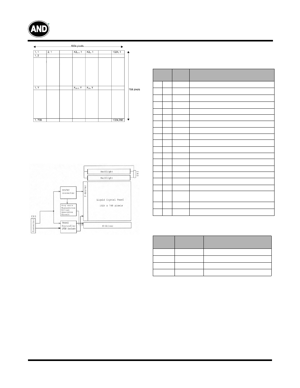
Block Diagram
Connector Pin Assignment for Interface
CN1 Input Signal
(see Notes below)
DF19L-20P-1H / Hirose Electric Co., Ltd.
Terminal
No.
Symbol
Function
1
V
DD
Power Supply: +3.3V
2
V
DD
Power Supply: +3.3V
3
V
SS
Ground
4
V
SS
Ground
5
RxIN0-
Neg. LVDS differential data input (R0-R5, G0)
6
RxIN0+ Pos. LVDS differential data input (R0-R5, G0)
7
V
SS
Ground
8
RxIN1-
Neg. LVDS differential data input (G1-G5, B0-B1)
9
RxIN1+
Pos. LVDS differential data input (G1-G5, B0-B1)
10
V
SS
Ground
11
RxIN2-
Neg. LVDS differential data input (B1-B5,HS,VS,DE)
12
RxIN2+
Pos. LVDS differential data input (B1-B5,HS,VS,DE)
13
V
SS
Ground
14
CLK-
Clock Signal (-)
15
CLK+
Clock Signal (+)
16
V
SS
Ground
17
U/D
Vert. Rev. (“L” level or Open; Normal, “H” level: Rev.)
18
L/R
Horiz. Rev. (“L” level or Open; Normal, “H” level:
Rev.)
19
V
SS
Ground
20
V
SS
Ground
CN2 CCFL Power Source
BHR-04VS-1/Japan Solderless Terminal Mfg. Co., Ltd
Terminal
No.
Symbol
Function
1
VFLH1
CCFL Power Supply (High Voltage)
2
VFLH2
CCFL Power Supply (Low Voltage)
3
NC
Non Connection (open)
4
VFLL
CCFL Power Supply (Low Voltage)
1) Drivers are fabricated on the LCD glass
2) Connector
s
CN1: DF19L-20P-1H / Hirose Electric Co., Ltd.
Mating Connector - DF19G-20S-1F (FPC) /
CN2: BHR-04VS-1/Japan Solderless Terminal Mfg. Co., Ltd.
Mating Connector - SM04(4.0)B-BHS-1 / JST
Notes:
Please connect GND pin to ground. Don’t use it as no-connect nor
connection with high impedance. NC terminal should be open. Take
away terminal No. 3 of the mating connector. If does not take away, it
may cause smoke burn of electrical parts by high voltage.
DF19G-20S-1C (Cable)
ANDpSi121GA0S-HB-KIT
