Connectors and jumpers list, Chapter 3, Board layout – Lanner LEC-7105 User Manual
Page 12
12
Board Layout
Chapter 3
Embedded and Industrial Computing
Connectors and Jumpers List
The tables below list the function of each of the board
jumpers and connectors by labels shown in the above
section. The next section in this chapter gives pin
definitions and instructions on setting jumpers.
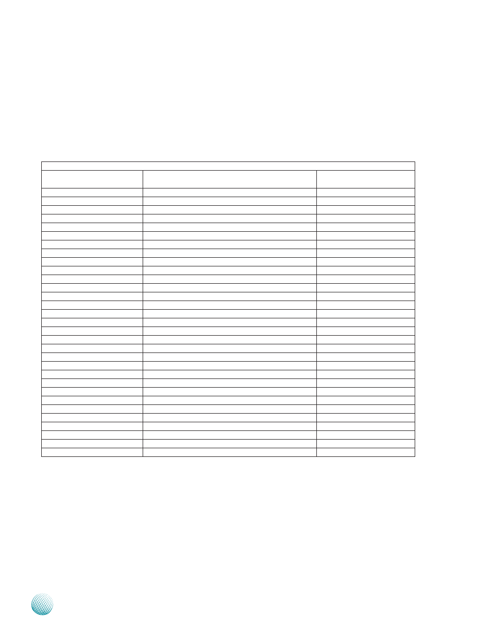
Table 3.1 Connector List for LEB-7105
Labels
Function
Pin Definition Reference
Page
CFD1
CompactFlash
P15
CN1 & CN2
Lineout Left/Right
P17
COM1
RS-232 Port
P14
COM2
RS-232/422/485 Port
P14
DIO1
Digital Input/Output
P15
DVI1
DVI-D Connector
P17
EUSB1
Power eSATA Port
P14
J1
SPI ROM Header
Reserved for Factory
J10
USB Pin Header
P16
J11
Miscellaneous Front Panel Pins
P16
J12
External Power Switch
P16
J13
SYSTEM Thermal Sensor
P17
J2
Line In/Out and MIC Pin Header
P17
J25
Mini-PCIe Power Voltage Selection
P17
J27
Power for Passive Antenna
P18
J3
SATA Power
P14
J6
ICH8M Chipset SMB Signals
Reserved for Factory
J7
LAN and WLAN LED (Only on MPCIE1)
P17
JP1 & JP2
Select COM1/COM2 Pin9 Function Jumper Settings
P14
JP3
Clean CMOS
P15
KBM1
PS/2 Keyboard and Mouse
P17
LAN1/LAN2 Ports
LAN1, LAN2 ports
P15
LPC1
Low Pin Count Bus for Debug Purpose
Reserved for Factory
MPCIE1
Mini-PCIe Slot (with SIM Card Reader)
P16
MPCIE2
Mini-PCIe Slot
P16
SATA1
Serial-ATA Connector 1
P14
SATA2
Serial-ATA Connector 2
P14
SCT1/SCT2
Seclect COM2 Protocol Jumper settings
P14
USB1
Dual USB Port
P16
USB2
Dual USB Port
P16
VGA
DB-15 VGA Port
P17