Chapter 3: motherboard information, Block diagram, Block diagram 7 – Lanner LEC-3000A User Manual
Page 9: Chapter 3, Motherboard information
7
Motherboard Information
Chapter 3
Embedded and Industrial Computing
Chapter 3:
Motherboard Information
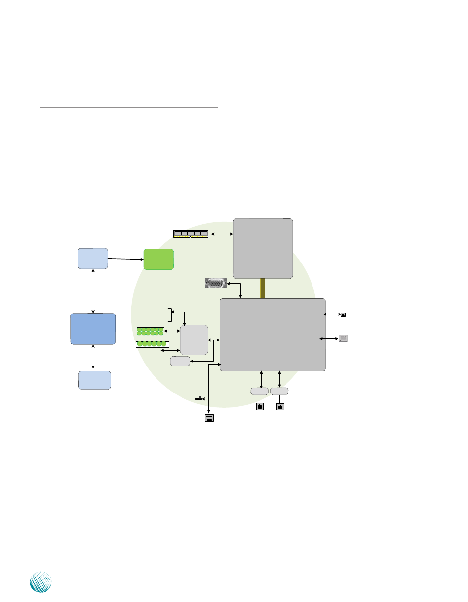
Block Diagram
The block diagram depicts the relationships among the
interfaces or modules on the motherboard Please refer
to the following figure for your motherboard’s layout
design
VIA C7®-M
processor
12 watts at 1.5GHz
VX800
(33X33mm)
~5W
LP
C
DDR2 667 MHz
800/400MHz FSB
Compact Flash
2x USB
PIN header
4x USB
connectors
U
SB
2
.0
S
A
TA
II
1x SATAII Port
Up to 2GB Maximum
Fintek
81865F
4 COM ports
Flash
BIOS
ID
E
VX800 integrated graphic
engine
VGA connector
Watchdog
LEB-3000A
DI/DO
Hardware Monitor
2x GbE RJ-45
Connectors w/ LED
2x PCI-E
RealTek
RTL8111
RealTek
RTL8111
VIA
D
riv
eS
ta
tio
n
PWM Module
DC +12V
Output
DC
+12~36V
DC +12V
Input
LEK-DC01
DC/DC Converter Board