Chapter 3, Board layout, Connectors and jumpers list – Lanner LVC-5550S User Manual
Page 14
14
Board Layout
Chapter 3
Embedded and Industrial Computing
Connectors and Jumpers List
The tables below list the function of each of the board
jumpers and connectors by labels shown in the above
section. The next section in this chapter gives pin
definitions and instructions on setting jumpers.
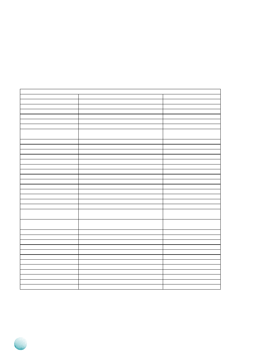
Table 3.1 Connector List for LVB-5550
Labels
Function
Pin Definition Reference Page
3GAUDC1
3G voice MIC-in and ear out connector
P18
AUDIO1
Line out and MIC-in audio connector
P16
CCMOS1
Clear CMOS jumper
P16
CF1
CompactFlash connector
P16
CN1
External power button connector
P17
CN2
204 Pin DDR3 SO-DIMM Socket
CN4
External RS-232 programming connector for
the MCU
P19
CN6
12V DC power-out connector
P17
COM1
COM Port 1
P15
COM2
COM Port 2
P15
COM3
COM Port 3
P15
CON2
2.5" SATA HDD power connector
P15
DC_IN1
9V~30V DC power-in connector with ignition P16
DGIOC1
6bit Digital Input/Output
P16
DLPC1
LPC port 80 debugging port
Reserved for factory use
DVI1
DVI-D connector
P17
JSPIROM1
SPI ROM BIOS downloading cable connector Reserved for factory use
KM1
PS/2 keyboard and mouse
P16
LANB1/LANB2
RJ-45 port with LED indicator
P17
LED1
Power LED and HDD LED
P18
LED2
Wi-Fi LED and 3G Wi-Fi LED
P18
LVDSC1
18bits LVDS connector with USB signal and
power button
P18
MCARD1
PCIe connector for Sierra 3G USB type Wi-Fi
module
P18
MPCIE1/2
1x mini PCIe connector (Version 1.2)
P17
PCOM1/2/3
Select COM1/COM2/COM3 Pin 9 function
P15
PSBTN1
Power button
P18
RSTSW1
System reset button
P18
SATA1
SATA connector
P15
SW1,SW2
Select MCU function
P19
SW3
Enable/disable COM1 termination
P15
SW4
Select COM1 type
P15
SW5
Select COM2 type
P15
SW6
Enable/disable COM2 termination
P15
USB1/USB2
USB port
P16
VGA1
VGA1 connector
P17