Installation, Supplied materials, Unit configuration – Verilink 400 (34-00222) Product Manual User Manual
Page 8
8
9
2.
Installation
This chapter contains information and instructions required to prepare the TxPORT
400 DSU/CSU for use. Included are configuration guidelines and connection
instructions.
Supplied Materials
Each 400 unit is shipped with the TxPORT 400 DDS DSU/ CSU reference manual.
You may require additional items for the installation and operation of the unit. Refer
to page 7 for complete ordering information.
Unit Configuration
On power up, each unit is configured to the hardware settings of the option switches
(S1). Subsequent changes to these settings will not take effect until the unit has been
reset. This may be accomplished either by removing and then reapplying power or
by pushing the test switch toward local loop LL and then quickly back to center or
NORM. The unit then recycles through its LEDs and reads the new configuration.
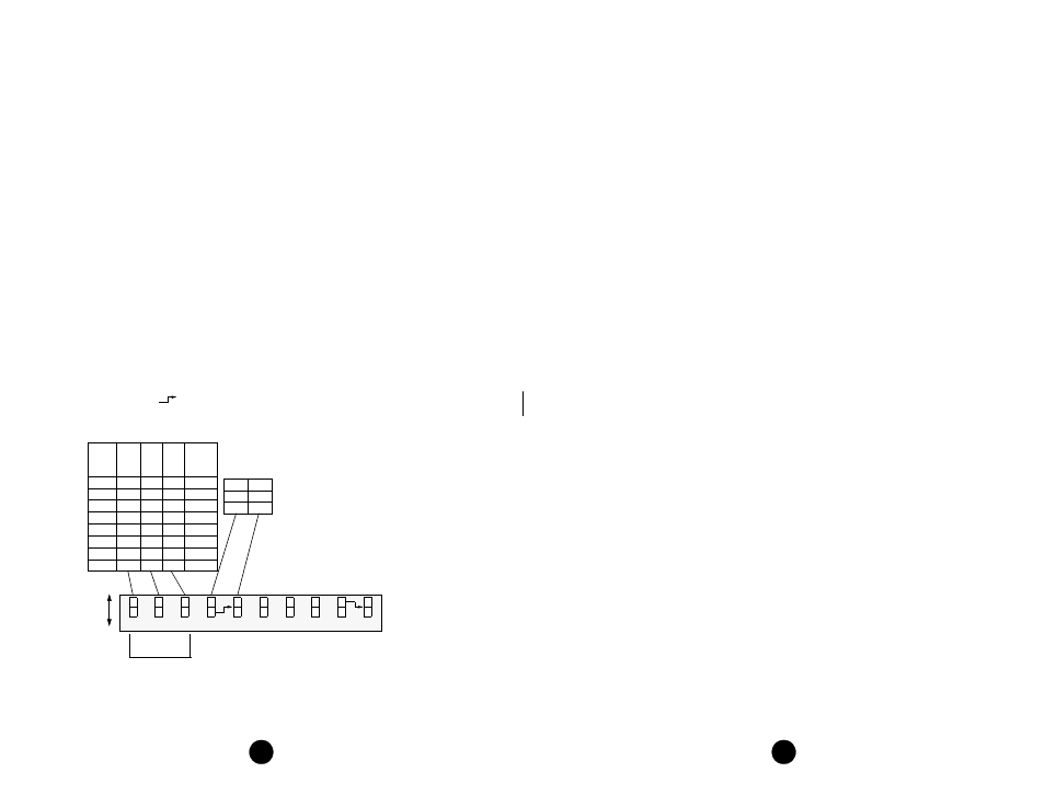
S1 is a 10-position DIP switch located on the unit’s rear panel. This switch provides
the following configuration parameters.
The symbol ‘
’ indicates that the switch pointed to is not functional unless
the opposite end of the arrow is in the position shown. For example, S1-5 is
not functional unless S1-4 is in the B position.
6
5
4
3
1
7
9
8
2
Da
ta
P
o
la
rit
y
C
irc
uit A
ssu
ra
nc
e
R
T
S
/CT
S
Cont
rol
Da
ta
P
o
la
rit
y
Circuit
As
su
rance
R
T
S
Nor
m
al
Delay
Channel
Bit Rate
A
B
V
.54 L
oop
V
.54 L
o
op
Int
er
n
al C
lock
L
ine C
lock
In
v
er
te
d
Nor
m
al
Of
f
On
En
ab
le
d
Inhi
bited
R
T
S
/CTS
Con
tr
o
l
R
T
S Contr
o
l
On
RT
S
->
C
T
S
D
el
ay
X 2
RT
S
->
C
T
S
D
el
ay
Nor
m
al
B
A
A
n/a
Master
Network
B
B
External
10
Rate
(kbps)
S1-1 S1- 2 S1- 3
RTS
to CTS
Delay
2.4
B
B
B
8 ms
4.8
A
B
B
4 ms
9.6
B
A
B
2 ms
19.2
A
A
B
1 ms
28 B
B
A
.8
ms
38.4 A
B
A
.5
ms
56 B
A
A
.4
ms
64 A
A
A
.3
ms
Channel Bit Rate Select: Positions S1-1, S1-2, and S1-3 select the channel bit
rate. Refer to the table in the above diagram to determine the switch settings for a
particular bit rate. The RTS to CTS delays are multiplied by two when position S1-
10 is in the B position.
Line Clock: Position S1- 4 selects either an internal clocking source or a loop tim-
ing source from the received data.
A - Loop timing source
B - Internal line clock
Internal Clock: Position S1-5 selects either the DSU external clock input or the
crystal oscillator as the clocking source. This function is applicable only if position
S1-4 is in the B position.
A - Internal master clock
B - DSU external clock input
V.54 Loop Operation: Position S1-6 enables or disables V.54 loop operation.
A - Disabled
B - Enabled
Data Polarity: Position S1-7 determines whether data bits are inverted. In the A
position, marks equal pulses. In the B position, spaces equal pulses. Receipt of OOF,
OOS, idle, or loop codes forces the DSU data to all marks (A position) or spaces (B
position).
A - Normal
B - Inverted
Circuit Assurance: When position S1-8 is On, the status of CF (receive line signal
detector) and CA (request to send) controls the output CB (clear to send). If either
CA or CF is Off (position A), CB is Off. If CA and CF are On (position B), CB is
On.
A - Off
B - On
RTS/CTS Control: When position S1-9 is in the B position, CTS is forced On
regardless of the RTS input status. In the A position, the delays are determined by
S1-10.
A - Normal Delay
B - Control On
RTS -> CTS Delay: When position S1-10 is in the A position, the RTS to CTS
delay is as shown in the S1-1, S1-2, and S1-3 bit rate table. In the B position, the
delays shown are multiplied by two.
A - Normal Delay
B - Delay multiplied by two
✍