Sundance SMT111 User Manual
Page 10
User Manual SMT111
Page 10 of 18
Last Edited: 21/05/2010 16:53:00
4.2.3 Quad UART
An Oxford Semiconductor 16C954 UART provides four RS232 channels.
Some Maxim MAX3241 devices perform the conversion from 3.3V LVTTL to true
RS232 signal levels.
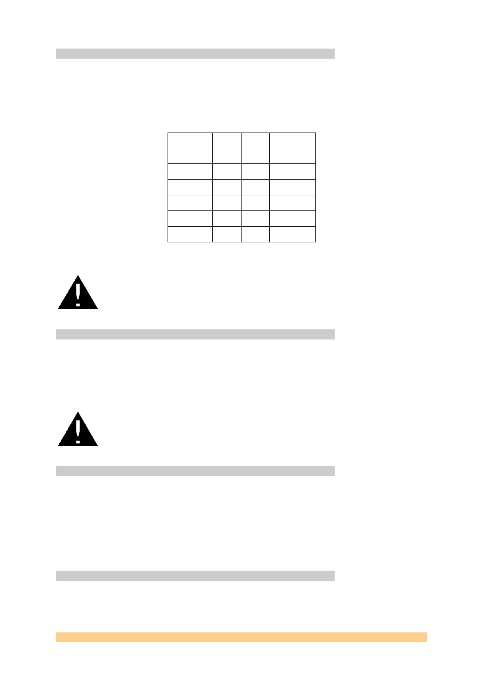
The RS232 signals are available via latching IDC headers. The pin-out is shown here:
Signal Pin Pin Signal
DCD 1 2 RX
TX 3 4 DTR
GND 5 6 DSR
RTS 7 8 CTS
RI 9
10 -
Table 2: RS232 – Pinout
The 10 pin IDC headers do NOT have the standard pinout required for a
direct connection to a 9-way D-type connector.
4.2.4 Flash memory device
The Xilinx Spartan-3 FPGA is coupled to a 64Mbytes of flash to enable configuration
of FPGA-only modules, or to store DSP applications and additional FPGA
configuration files (bitstreams).
A separate MicroSD (Transflash) socket connects directly to the FPGA.
No FPGA IP core is provided as standard. However with the addition of
a MicroBlaze processor, a full FAT file system may be implemented.
4.2.5 JTAG_IN and JTAG_OUT (LVTTL I/Os) connectors
An XDS510/560 compatible 14-way 0.1” pitch DIL pin header is provided to enable
debugging of a DSP module using Texas Instruments Code Composer Studio.
A JTAG_OUT connector can be used to chain this carrier with any other Sundance
carrier board. JTAG chaining is handled by the Xilinx FPGA.
The JTAG_OUT connector can be used to carry general purpose LVTTL I/O signals.
The selection of JTAG_OUT or LVTTL_I/Os is made by a DIP switch (SW1).