Functional block diagram, Udc-163 block diagram, One dual-rate hd/sd-sdi. outputs – Sierra Video UDC-163 User Manual
Page 7: Four reclocked hd/sd-sdi copies of the input
UDC-163 User Manual
(V 1.2)
Page 7 of 31
The UDC-163 also preserves several key non video signals across a downconversion or ARC.
Embedded audio is de-embedded at the input, delayed appropriately, and then embedded at the output
in the new format. Timecode signals (as VITC or as in SMPTE RP-188) are extracted, delayed the
appropriate amount, and then embedded in the output video. Standard definition closed captioning data
(NTSC Line 21) is decoded, delayed, and embedded in the output video, regardless of aspect ratio
correction.
The product also provides full color proc control of the output video, with separate controls for Gain,
Lift, Saturation and Color Phase.
The input and outputs of the UDC-163 are the following:
Input:
One dual-rate HD/SD-SDI.
Outputs:
Four reclocked HD/SD-SDI copies of the input.
Four user selectable (SD-SDI or Composite) down-converted HD or SD ARC’d outputs.
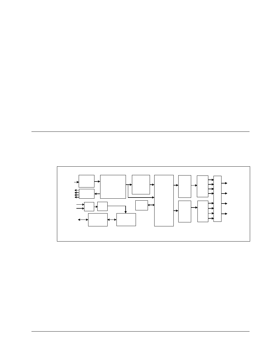
Functional Block Diagram
The UDC-163 has a very flexible signal flow path and feature set that combines several products into
one compact package. To understand its capabilities, this section reviews the basic structure of the
UDC-163.
Figure 1. Simplified Block Diagram of UDC-163 Functions
Starting in the upper left of the block diagram, the dual-rate (HD/SD) serial digital signal is equalized,
reclocked and then deserialized. A reclocked copy of the input is driven out of four BNCs (3, 4, 5, and
6). Once deserialized, the video standard and frame rate is determined.
Coming out of the deserializer, the parallel video data path goes to the image scalar circuitry, where it
is down, aspect and/or frame rate converted depending on the signal input and user settings. After
conversion audio, timecode, and closed captioning signals are embedded. Finally the reticule overlays
(if any) are applied, and the signal passes through circuitry to reduce output clock jitter.
HD/SD
Input
Dual
Rate
Input Eq.
Dual Rate
Reclock,
Decode and
De-serialize
SD
Serializer
SD
Encoder
SD
Analog
Output
SD-SDI
Output
Path
Routing
Reticule
Overlay
Analog
Composite
or
SD
Driver
Micro-
processor
Remote
I/O
Frame
Controller
UDC-163
Block Diagram
and
Down
Conversion
and ARC
Sync
Detect
Reference
Input
Re-clocked
Outputs
Input
Copies
SW
TCP-IP
Audio
Memory
Sel.
SW