Circuit description, Hdda 1x9 digital video path block diagram – Sierra Video HDA-109 User Manual
Page 22
SIERRA VIDEO
16
Circuit Description
Please refer to the Block Diagram and the schematic when reading the circuit description.
Cable
EQ
Re-Clocker
J3
J5
J7
J9
J4
J6
J8
J10
J1
Dual
Output
Driver
1
Dual
Output
Driver
2
Dual
Output
Driver
3
Dual
Output
Driver
4
/RESET_1
SCL
SDA
SDO+
SDO2+
SDO+
SDO+
SDO+
SDO+
SDO1+
SDO1+
SDO1+
SDO1+
SD/HD
SD/HD__SLEW
PLL_LOCK
/CD
EQ_BYPASS
EQ_MUTE
RATE0/1
RECLK_BYPASS
RECLK_MUTE
/RSTO_4
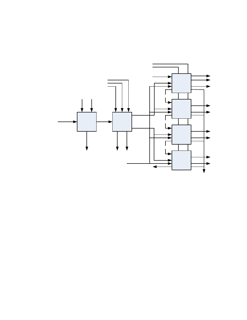
HDDA 1X9
DIGITAL VIDEO PATH
BLOCK DIAGRAM
/FAULT
/RESET
/RESET
/RESET
J2
SDO-
(INVERTED
OUTPUT)
The digital path is made up of three active components. First a cable EQ stage that
automatically corrects for the loss over frequency that is caused by the cable attached to
the input. The equalized serial stream is then differentially connected to a re-clocker that
derives a clock from the data stream and then re-clocks the data stream. There can be
either two re-clocked data streams at the out of the re-clocker or one data stream and
one clock out of the re-clocker. We are using both outputs as data streams so that each
output can drive just two output drivers thus reducing the length of the line that the re-
clocker would have to drive and improving the matching to the PCB diff pair. Each output
driver has two differential outputs but we only use the positive output from each
differential pair because one of the requirements is that we must be able to pass
ASI/DVB signals which cannot tolerate phase inversions of its data stream. We are using
3G parts throughout that can handle 270Mb to 3G which will make it an all purpose re-
clocking DA.
A new rear module that has improved 3G characteristics is used that has a connector
that looks the same as all other openGear boards but has closer spacing between pins
and better high frequency performance.