0 control & data registers – Measurement Computing PC104-DO48H User Manual
Page 11
5.0 CONTROL & DATA REGISTERS
Each PC104-DO48 is composed of parallel output chips. Each address contains one
latch and one buffer controlling eight output pins. The ports are arranged in sets of
three, with an intervening NA (not used) address. This scheme allows compatibility
with software written to control 82C55 based boards when the 82C55 is used as all
outputs. On those boards every fourth address contains a control register.
The first address, or BASE ADDRESS, is determined by setting a bank of switches on
the board.
To write a control data to an output register, the individual bits must be set to 0 or 1
then combined to form a Byte.
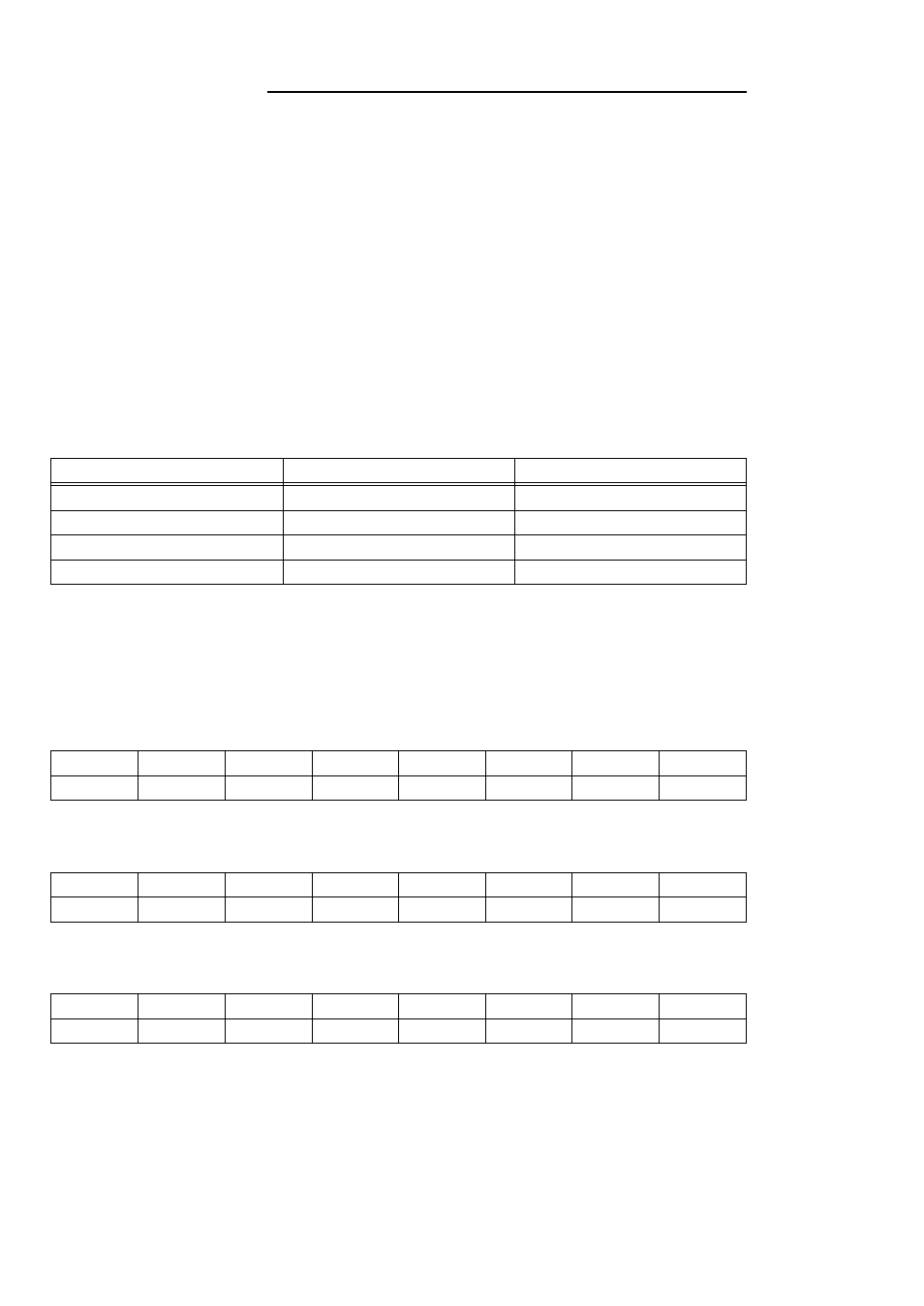
The registers and their function are listed on the following table.
None
None
BASE + 3, 7
Port C Output
None
BASE + 2, 6
Port B Output
None
BASE + 1, 5
Port A Output
None
BASE + 0, 4
WRITE FUNCTION
READ FUNCTION
ADDRESS
There are two sets of digital output lines. Each set has 24 outputs that are divided into
three ports of eight lines each. An 8-bit register accesses each port. The register
addresses are given in the table above and the bit maps below.
PORT A DATA
BASE ADDRESS + 0, 4
A0
A1
A2
A3
A4
A5
A6
A7
0
1
2
3
4
5
6
7
PORT B DATA
BASE ADDRESS + 1, 5
B0
B1
B2
B3
B4
B5
B6
B7
0
1
2
3
4
5
6
7
PORT C DATA
BASE ADDRESS + 2, 6
C0
C1
C2
C3
C4
C5
C6
C7
0
1
2
3
4
5
6
7
7