Chapter 3 – DFI KB968 User Manual
Page 23
www.dfi .com
Chapter 3 Hardware Installation
23
Chapter 3
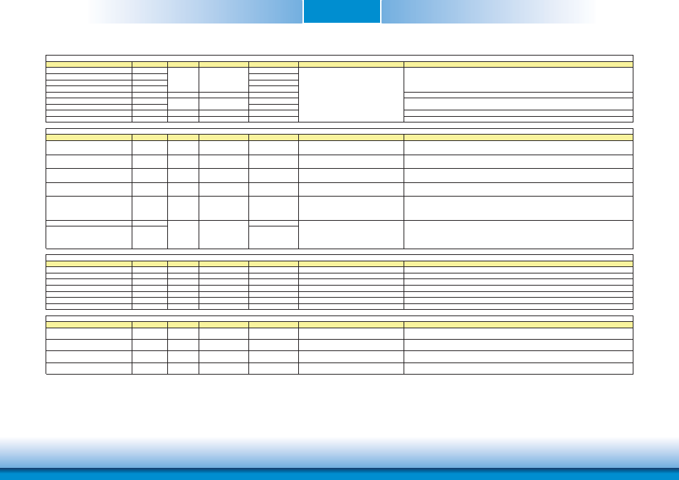
Signal
Pin#
Pin Type
Pwr Rail /Tolerance
KB968
Carrier Board
Description
LPC_AD0
B4
LPC_AD1
B5
LPC_AD2
B6
LPC_AD3
B7
LPC_FRAME#
B3
O CMOS
3.3V / 3.3V
LPC frame indicates the start of an LPC cycle
LPC_DRQ0#
B8
LPC_DRQ1#
B9
LPC_SERIRQ
A50
I/O CMOS
3.3V / 3.3V
PU 40-50K to 3.3V
LPC serial interrupt
LPC_CLK
B10
O CMOS
3.3V / 3.3V
LPC clock output - 33MHz nominal
Signal
Pin#
Pin Type
Pwr Rail /Tolerance
KB968
Carrier Board
Description
SPI_CS#
B97
O CMOS
3.3V Suspend/3.3V
Connect a series resistor 33ȟ to Carrier
Board SPI Device CS# pin
Chip select for Carrier Board SPI - may be sourced from chipset SPI0 or SPI1
SPI_MISO
A92
I CMOS
3.3V Suspend/3.3V
Connect a series resistor 33ȟ to Carrier
Board SPI Device SO pin
Data in to Module from Carrier SPI
SPI_MOSI
A95
O CMOS
3.3V Suspend/3.3V
Connect a series resistor 33ȟ to Carrier
Board SPI Device SI pin
Data out from Module to Carrier SPI
SPI_CLK
A94
O CMOS
3.3V Suspend/3.3V
Connect a series resistor 33ȟ to Carrier
Board SPI Device SCK pin
Clock from Module to Carrier SPI
SPI_POWER
A91
O
3.3V Suspend/3.3V
Power supply for Carrier Board SPI – sourced from Module – nominally
3.3V. The Module shall provide a minimum of 100mA on SPI_POWER.
Carriers shall use less than 100mA of SPI_POWER. SPI_POWER
shall only be used to power SPI devices on the Carrier
BIOS_DIS0#
A34
BIOS_DIS1#
B88
Signal
Pin#
Pin Type
Pwr Rail /Tolerance
KB968
Carrier Board
Description
VGA_RED
B89
O Analog
Analog
PD 150R to GND
PD 150R
Red for monitor. Analog output
VGA_GRN
B91
O Analog
Analog
PD 150R to GND
PD 150R
Green for monitor. Analog output
VGA_BLU
B92
O Analog
Analog
PD 150R to GND
PD 150R
Blue for monitor. Analog output
VGA_HSYNC
B93
O CMOS
3.3V / 3.3V
PD 1K to GND
Horizontal sync output to VGA monitor
VGA_VSYNC
B94
O CMOS
3.3V / 3.3V
Vertical sync output to VGA monitor
VGA_I2C_CK
B95
I/O OD CMOS 3.3V / 3.3V
PU 4.7K to 3.3V
DDC clock line (I2C port dedicated to identify VGA monitor capabilities)
VGA_I2C_DAT
B96
I/O OD CMOS 3.3V / 3.3V
PU 4.7K to 3.3V
DDC data line.
Signal
Pin#
Pin Type
Pwr Rail /Tolerance
KB968
Carrier Board
Description
SER0_TX
A98
O CMOS
5V/5V
PD 4.7K
General purpose serial port 0 transmitter
SER0_RX
A99
I CMOS
3.3V/5V
PU 47K to 3.3V
General purpose serial port 0 receiver
SER1_TX
A101
O CMOS
5V/5V
PD 4.7K
General purpose serial port 1 transmitter
SER1_RX
A102
I CMOS
3.3V/5V
PU 47K to 3.3V
General purpose serial port 1 receiver
3.3V / 3.3V
LPC serial DMA request
I/O CMOS
3.3V / 3.3V
VGA Signals Descriptions
NA
Selection straps to determine the BIOS boot device.
The Carrier should only float these or pull them low, please refer to
COM Express Module Base Specification Revision 2.1 for strapping options of BIOS disable signals.
LPC Signals Descriptions
Serial Interface Signals Descriptions
I CMOS
I CMOS
LPC multiplexed address, command and data bus
SPI Signals Descriptions
Connect to LPC device