Table 5-1, Clock structure – Artesyn SCP-P4040-4G-ENP2 Installation and Use (August 2014) User Manual
Page 56
Clock Structure
SCP-P4040-4G-ENP2 Installation and Use (6806800P60B)
56
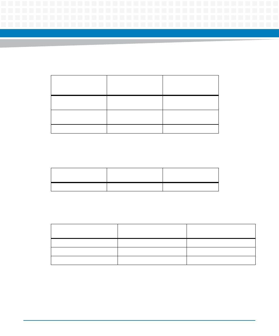
For ruggedized variant where dip switches are not mounted, the following signals connects to
COM Express connector and will be up to carrier to configure them:
For standard commercial variant where dip switches are populated, the frequency of all the
three SERDES banks' reference clock is selectable between 100MHz and 125MHz by three bits
of switcher S1.
It can also be set by three GPIOs, referring to the following table:
The setting of these three bits of S1 or GPIOs depends on the protocols running at the SERDES
lanes of each bank. When the SERDES lanes are running at the speed of 3.125 Gbps, then the
corresponding bank reference clock should be set as 125 MHz, and at the speed besides 3.125
Gbps, it should be set as 100 MHz. For example, if lanes in bank 1 are configured as PCIE, then
the bank 1 reference clock should be set as 100 MHz, and if XAUI, then should be set as 125
MHz.
SERDES bank 1
reference clock select
(pin B97 on COME)
SERDES bank 2
reference clock select
(pin B98 on COME)
SERDES bank 3
reference clock select
(pin B99 on COME)
Bank1_SEL_FS0=0,
100MHz
Bank2_SEL_S1=0,
100MHz
Bank2_SEL_S1=0,
100MHz
Bank1_SEL_FS0=1,
125MHz
Bank2_SEL_S1=1,
125MHz
Bank2_SEL_S1=1,
125MHz
*Default:100MHz
*Default:125MHz
*Default:125MHz
SERDES bank 1
reference clock
SERDES bank 2
reference clock
SERDES bank 3
reference clock
Default:100MHz
Default:125MHz
Default:125MHz
Table 5-1 Configuration of the frequency of SERDES reference clock by GPIO
SERDES bank 1 reference
clock
SERDES bank 2 reference clock SERDES bank 3 reference clock
CPU_GPIO23=0, 100MHz
CPU_GPIO24=0, 100MHz
CPU_GPIO26=0, 100MHz
CPU_GPIO23=1, 125MHz
CPU_GPIO24=1, 125MHz
CPU_GPIO26=1, 125MHz
Default:100MHz
Default:125MHz
Default:125MHz