2 component locations – Aplex Technology APC-3081 User Manual
Page 19
APC-3081 User Manual
19
Pin47, EN_3V_5V_S5, CPU board send an auxiliary power supply signal to IO baseboard for
operating.
Pin49, SMC_ONOFF #, IO baseboard send to CPU board to issue a system ON/ OFF signal;
Pin51, 3V_5V_S5_OK, IO baseboard issued confirmed auxiliary power OK signal to CPU board;
Pin53, SMC_LATCH #, CPU board sent disable system signal to the IO baseboard;
Pin57, CPU_THERMDA, Defined the thermal diode positive signal to CPU board;
Pin59, CPU_THERMDC, Defined the thermal diode negative signal to CPU board;
Pin89, SIO_PWROK, IO baseboard send to the power OK signal to CPU board;
Pin91, USB2_CLIENT_EN, USB2_CLIENT signal enable, but also can be defined as GPIO;
Pin93, from the US15W access via CPLD out as defined GPIO;
Pin95, Software Reset signal, active low;
Pin97, AT Power Mode allows signal, active low;
Pin100, SCH_SPKR, CPU board sent to the buzzer signal- sound to IO baseboard
2.1.7.10 LVDS panel backlight signal
The main different functions of Rev: 1.20 version and Rev: 1.30 version is the CN2 added LVDS
backlight
control screen signals.
Pin 96 L_BKLEN, is defined for Backlight start signal;
Pin 98 L_BKLCTRL, is defined for backlight brightness control signal.
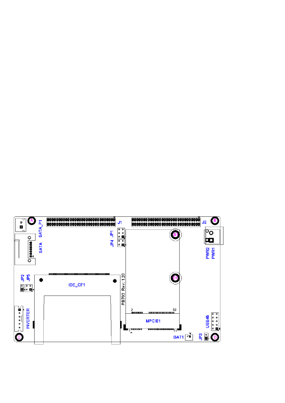
2.2 Component Locations
Figure 2.3: PB-703 Baseboard Overview